User’s Manual
IBM PowerPC 750GX and 750GL RISC Microprocessor
PowerPC 750GX Overview
Page 36 of 377
gx_01.fm.(1.2)
March 27,2006
The address and data buses operate independently. Address and data tenures of a memory access are
decoupled to provide more flexible control of bus traffic. The primary activity of the system interface is trans-
ferring data and instructions between the processor and system memory. There are two types of memory
accesses:
The 750GX also supports address-only operations, which are variants of the burst and single-beat operations
(for example, atomic memory operations and global memory operations that are snooped), and address retry
activity (for example, when a snooped read access hits a modified block in the cache). The broadcast of
some address-only operations is controlled through the address broadcast enable bit (HID0[ABE]). I/O
accesses use the same protocol as memory accesses.
Access to the system interface is granted through an external arbitration mechanism that allows devices to
compete for bus mastership. This arbitration mechanism is flexible, allowing the 750GX to be integrated into
systems that implement various fairness and bus-parking procedures to avoid arbitration overhead.
Typically, memory accesses are weakly ordered—sequences of operations, including load/store string and
multiple instructions, do not necessarily complete in the order they begin. This maximizes the efficiency of the
bus without sacrificing data coherency. The 750GX allows read operations to go ahead of store operations
except when a dependency exists, or when a noncacheable access is performed. It also allows a write oper-
ation to go ahead of a previously queued read data tenure (for example, letting a snoop push be enveloped
between address and data tenures of a read operation). Because the 750GX can dynamically optimize run-
time ordering of load/store traffic, overall performance is improved.
The system interface is specific for each PowerPC microprocessor implementation.
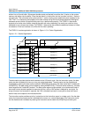
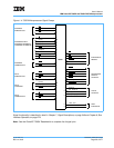
The 750GX signals are grouped as shown in Figure 1-3, System Interface. Test and control signals provide
diagnostics for selected internal circuits.
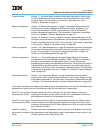
Single-beat transfers Allow transfer sizes of 8, 16, 24, 32, or 64 bits in one bus clock cycle. Single-beat
transactions are caused by uncacheable read and write operations that access
memory directly when caches are disabled, for cache-inhibited accesses, and for
stores in write-through mode. The two latter accesses are defined by control bits
provided by the MMU during address translation.
4-beat burst (32-byte)
data transfers
Burst transactions, which always transfer an entire cache block (32 bytes), are initi-
ated when an entire cache block is transferred. If the caches on the 750GX are
enabled and using write-back mode, burst-read operations are the most common
memory accesses, followed by burst-write memory operations.


