


101
CHAPTER 5 CPU ARCHITECTURE
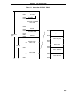
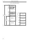
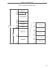
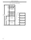
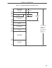
5.1.5 Data memory addressing
The method to specify the address of the instruction to be executed next, or the address of a register or memory
to be manipulated when an instruction is executed is called addressing.
The address of the instruction to be executed next is addressed by the program counter PC (for details, refer to
5.3 Instruction Address Addressing).
To address the memory that is manipulated when an instruction is executed, the
µ
PD78054, 78054Y Subseries
is provided with many addressing modes with a high operability. Especially at addresses corresponding to data
memory area, particular addressing modes are possible to meet the functions of the special function registers (SFRs)
and general registers. This area is between FD00H and FFFFH for the
µ
PD78052 and 78052Y, and between FB00H
and FFFFH for the
µ
PD78053, 78053Y, 78054, 78054Y, 78P054, 78055, 78055Y, 78056, 78056Y, 78058, 78058Y,
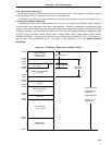
78P058, and 78P058Y. The data memory space is the entire 64K-byte space (0000H to FFFFH). Figure 5-9 to 5-16
show the data memory addressing modes. For details of each addressing, refer to 5.4 Operand Address
Addressing.
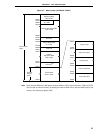
Figure 5-9. Data Memory Addressing (
µ
PD78052, 78052Y)
0000H
General Registers
32 × 8 bits
Internal ROM
16384 × 8 bits
Internal Buffer RAM
32 × 8 bits
External Memory
47744 × 8 bits
Reserved
4000H
3FFFH
FA80H
FA7FH
FAC0H
FABFH
FAE0H
FADFH
FEE0H
FEDFH
FF00H
FEFFH
FFFFH
Internal High-speed RAM
512 × 8 bits
Reserved
FD00H
FCFFH
FF20H
FF1FH
FE20H
FE1FH
Special Function
Registers (SFRs)
256 × 8 bits
SFR Addressing
Register Addressing
Short Direct
Addressing
Direct Addressing
Register Indirect
Addressing
Based Addressing
Based Indexed
Addressing