


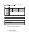

166
CHAPTER 7 CLOCK GENERATOR
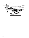
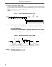
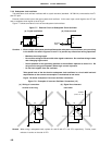
IC X2 X1
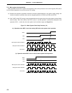
7.4.2 Subsystem clock oscillator
The subsystem clock oscillator oscillates with a crystal resonator (standard: 32.768 kHz) connected to the XT1
and XT2 pins.
External clocks can be input to the main system clock oscillator. In this case, input a clock signal to the XT1 pin
and an antiphase clock signal to the XT2 pin.
Figure 7-7 shows an external circuit of the subsystem clock oscillator.
Figure 7-7. External Circuit of Subsystem Clock Oscillator
(a) Crystal oscillation (b) External clock
Remark When using a subsystem clock, replace X1 and X2 with XT1 and XT2, respectively. Further, insert
resistors in series on the side of XT2.
X2 X1
PORTn
(n=0-7, 12, 13)
IC
External
Clock
XT2
XT1
PD74HCU04
µ
XT2
XT1
32.768
kHz
IC
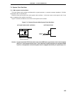
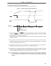
Cautions 1. When using a main system clock oscillator and a subsystem clock oscillator, carry out wiring
in the broken line area in Figures 7-6 and 7-7 to prevent any effects from wiring capacities.
• Minimize the wiring length.
• Do not allow wiring to intersect with other signal conductors. Do not allow wiring to come
near changing high current.
• Set the potential of the grounding position of the oscillator capacitor to that of VSS. Do
not ground to any ground pattern where high current is present.
• Do not fetch signals from the oscillator.
Take special note of the fact that the subsystem clock oscillator is a circuit with low-level
amplification so that current consumption is maintained at low levels.
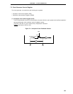
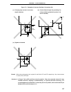
Figure 7-8 shows examples of incorrect oscillator connection.
Figure 7-8. Examples of Incorrect Oscillator Connection (1/2)
(a) Wiring of connection (b) Signal lines intersect
circuits is too long each other