


278
CHAPTER 14 A/D CONVERTER
14.5 A/D Converter Cautions
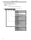
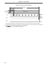
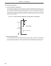
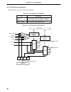
(1) Power consumption in standby mode
The A/D converter operates on the main system clock. Therefore, its operation stops in STOP mode or in
HALT mode with the subsystem clock. As a current still flows in the AVREF0 pin at this time, this current must
be cut in order to minimize the overall system power dissipation. In Figure 14-10, the power dissipation can
be reduced by outputting a low-level signal to the output port in standby mode. However, there is no precision
to the actual AV
REF0 voltage, and therefore the conversion values themselves lack precision and can only be
used for relative comparison.
Figure 14-10. Example of Method of Reducing Current Dissipation in Standby Mode
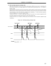
(2) Input range of ANI0 to ANI7
The input voltages of ANI0 to ANI7 should be within the specification range. In particular, if a voltage above
AV
REF0 or below AVSS is input (even if within the absolute maximum rating range), the conversion value for
that channel will be indeterminate. The conversion values of the other channels may also be affected.
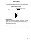
Series Resistor String
VDD
AVREF0
AVREF0 = VDD
AVSS
Output Port
.
.
µ
PD78054, 78054Y