


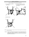
162
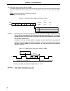
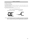
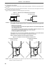
CHAPTER 7 CLOCK GENERATOR
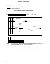
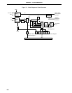
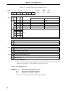
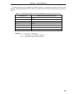
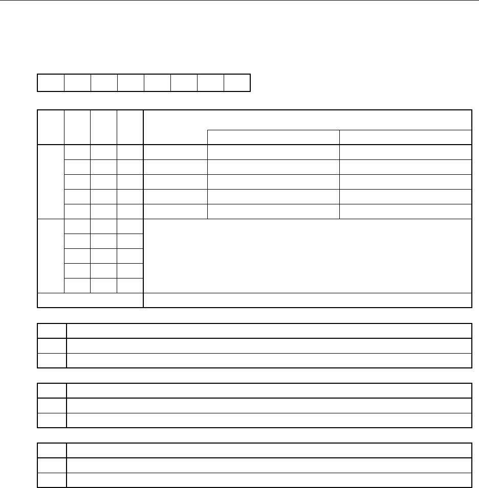
MCC FRC CLS CSS PCC2 PCC1 PCC0PCC
CLS
0
1
Main system clock
Subsystem clock
FFFBH 04H R/W
Note 1
<7> <5> <4>Symbol
Address
After
Reset R/W
0
<6> 3 2 0
1
CSS
0
0f
XX
/2
PCC2
CPU CIock (f
CPU
) Selection
PCC1 PCC0
CPU Clock Status
0
0
0
1
0
0
1
1
0
1
1
0
0
0
0
0
0
0
0
1
1
0
0
1
1
0
1
0
f
XX
/2
2
f
XX
/2
3
f
XX
/2
4
f
XT
/2
f
XX
Setting prohibitedOther than above
FRC
0
1
Internal feedback resistor used
Internal feedback resistor not used
Subsystem Clock Feedback Resistor Selection
MCC
0
1
Oscillation possible
Oscillation stopped
Main System Clock Oscillation Control
Note 2
R/W
R/W
R/W
R
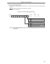
f
x
/2
f
x
/2
2
f
x
/2
3
f
x
/2
4
f
x
f
x
/2
2
f
x
/2
3
f
x
/2
4
f
x
/2
5
f
x
/2
MCS = 1 MCS = 0
0
1
Figure 7-3. Processor Clock Control Register Format
Notes 1. Bit 5 is Read Only.
2. When the CPU is operating on the subsystem clock, MCC should be used to stop the main
system clock oscillation. A STOP instruction should not be used.
Caution Bit 3 must be set to 0.
Remarks 1. f
XX : Main system clock frequency (fX or fX/2)
2. fX : Main system clock oscillator frequency
3. fXT : Subsystem clock oscillator frequency
4. MCS : Bit 0 of oscillation mode selection register (OSMS)