


568
CHAPTER 27 INSTRUCTION SET
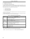
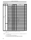
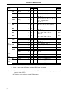
Clock Flag
Note 1 Note 2
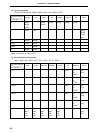
ZACCY
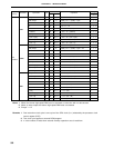
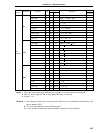
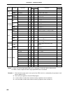
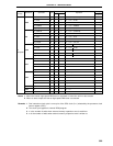
ADDW AX, #word 3 6 – AX, CY ← AX + word ×××
SUBW AX, #word 3 6 – AX, CY ← AX – word ×××
CMPW AX, #word 3 6 – AX – word ×××
MULU X 2 16 – AX ← A × X
DIVUW C 2 25 – AX (Quotient), C (Remainder) ← AX ÷ C
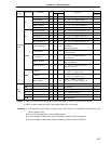
r12–r ← r + 1 ××
saddr 2 4 6 (saddr) ← (saddr) + 1 ××
r12–r ← r – 1 ××
saddr 2 4 6 (saddr) ← (saddr) – 1 ××
INCW rp 1 4 – rp ← rp + 1
DECW rp 1 4 – rp ← rp – 1
ROR A, 1 1 2 – (CY, A7 ← A0, Am – 1 ← Am) × 1 time ×
ROL A, 1 1 2 – (CY, A0 ← A7, Am + 1 ← Am) × 1 time ×
RORC A, 1 1 2 – (CY ← A0, A7 ← CY, Am – 1 ← Am) × 1 time ×
ROLC A, 1 1 2 – (CY ← A7, A0 ← CY, Am + 1 ← Am) × 1 time ×
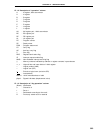
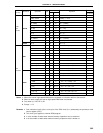
A3 – 0 ← (HL)3 – 0, (HL)7 – 4 ← A3 – 0,
(HL)3 – 0 ← (HL)7 – 4
A3 – 0 ← (HL)7 – 4, (HL)3 – 0 ← A3 – 0,
(HL)7 – 4 ← (HL)3 – 0
Decimal Adjust Accumulator after
Addition
Decimal Adjust Accumulator after
Subtract
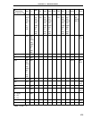
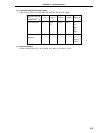
CY, saddr.bit 3 6 7 CY ← (saddr.bit) ×
CY, sfr.bit 3 – 7 CY ← sfr.bit ×
CY, A.bit 2 4 – CY ← A.bit ×
CY, PSW.bit 3 – 7 CY ← PSW.bit ×
CY, [HL].bit 2 6 7 + n CY ← (HL).bit ×
saddr.bit, CY 3 6 8 (saddr.bit) ← CY
sfr.bit, CY 3 – 8 sfr.bit ← CY
A.bit, CY 2 4 – A.bit ← CY
PSW.bit, CY 3 – 8 PSW.bit ← CY ××
[HL].bit, CY 2 6
8 + n + m
(HL).bit ← CY
Notes 1. When the internal high-speed RAM area is accessed or instruction with no data access.
2. When an area except the internal high-speed RAM area is accessed.
Remarks 1. One instruction clock cycle is one cycle of the CPU clock (f
CPU) selected by the processor clock
control register (PCC).
2. This clock cycle applies to internal ROM program.
3. n is the number of waits when external memory expansion area is read from.
4. m is the number of waits when external memory expansion area is written to.
Mnemonic Operands Byte Operation
Instruction
Group
INC
16-bit
operation
Increment/
decrement
DEC
Rotate
ROR4 [HL] 2 10
12 + n + m
ROL4 [HL] 2 10
12 + n + m
ADJBA 24 – ×××
ADJBS 24 – ×××
BCD
adjust
MOV1
Bit
manipulate
Multiply/
divide