


377
CHAPTER 17 SERIAL INTERFACE CHANNEL 0 (
µ
PD78054Y Subseries)
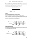
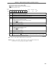
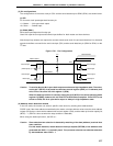
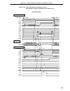
(5) Pin configurations
The configurations of the serial clock pin SCL and the serial data bus pins SDA0 (SDA1) are shown below.
(a) SCL
Pin for serial clock input/output dual-function pin.
<1> Master ..... N-ch open-drain output
<2> Slave ....... Schmitt input
(b) SDA0 (SDA1)
Serial data input/output dual-function pin.
Uses N-ch open-drain output and Schmitt-input buffers for both master and slave devices.
Note that pull-up resistors are required to connect to both serial clock line and serial data bus line, because
open-drain buffers are used for the serial clock pin (SCL) and the serial data bus pin (SDA0 or SDA1) on the
I
2
C bus.
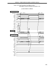
Figure 17-21. Pin Configuration
Caution To receive data, the N-ch open-drain output must be set to high-impedance state. Therefore,
set the bit 7 (BSYE) of the serial bus interface control register (SBIC) to 1 in advance, and
write FFH to the serial I/O shift register 0 (SIO0).
When the wake-up function is used (by setting the bit 5 (WUP) of the serial operating mode
register 0 (CSIM0)), however, do not write FFH to SIO0 before reception. Even if FFH is not
written to SIO0, the N-ch open-drain output is always in high-impedance state.
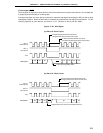
(6) Address match detection method
In the I
2
C mode, the master can select a specific slave device by sending slave address data.
CSIIF0 is set if the slave address transmitted by the master coincides with the value set to the slave address
register (SVA) when a slave device address has a slave register (SVA), and the wake-up function specify bit
(WUP) = 1 (CSIIF0 is also set when the stop condition is detected).
When using the wake-up function, set SIC to 1.
Caution Slave selection/non-selection is detected by matching of the data (address) received after
start condition.
For this match detection, match detection interrupt request (INTCSI0) of the address to be
generated with WUP = 1 is normally used. Thus, execute selection/non-selection detection
by slave address when WUP = 1.
V
DD
V
DD
SCL
SDA0(SDA1)
Master device
Clock output
(Clock input)
Data output
Data input
Slave devices
(Clock output)
Clock input
Data output
Data input
SCL
SDA0(SDA1)