


268
CHAPTER 14 A/D CONVERTER
(7) AVREF0 pin
This pin inputs the A/D converter reference voltage.
It converts signals input to ANI0 to ANI7 into digital signals according to the voltage applied between AV
REF0
and AVSS.
The current flowing in the series resistor string can be reduced by setting the voltage to be input to the AVREF0
pin to AVSS level in standby mode.
Caution A serial resistor string of approximately 10 kΩ is connected between the AVREF0 pin and the
AV
SS pin. Therefore, when the output impedance of the reference voltage is high, it is
connected in parallel to the serial resistor string between the AVREF0 pin and the AVSS pin
so that the reference voltage error increases.
(8) AV
SS pin
This is a GND potential pin of the A/D converter. Keep it at the same potential as the VSS pin when not using
the A/D converter.
(9) AV
DD pin
This is an A/D converter analog power supply pin. Keep it at the same potential as the V
SS pin when not using
the A/D converter.
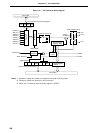
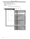
Caution AV
DD pin is the power supply pin of the analog circuit, and it supplies power also to the input
circuit of ANI0/P10 to ANI7/P17. Therefore, always supply the voltage of the same level as
VDD as shown in Figure 14-2 also in applications which switch to backup power supply.
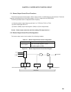
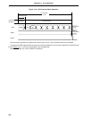
Figure 14-2. Handling of AV
DD Pin
Main
power
supply
AV
REF0
V
DD
AV
DD
AV
SS
V
SS
Capacitor
for back-up