Rev.1.02 Jul 01, 2005 page 238 of 314
REJ09B0126-0102
M16C/6N Group (M16C/6NL, M16C/6NN) 20. Flash Memory Version
Under development
This document is under development and its contents are subject to change.
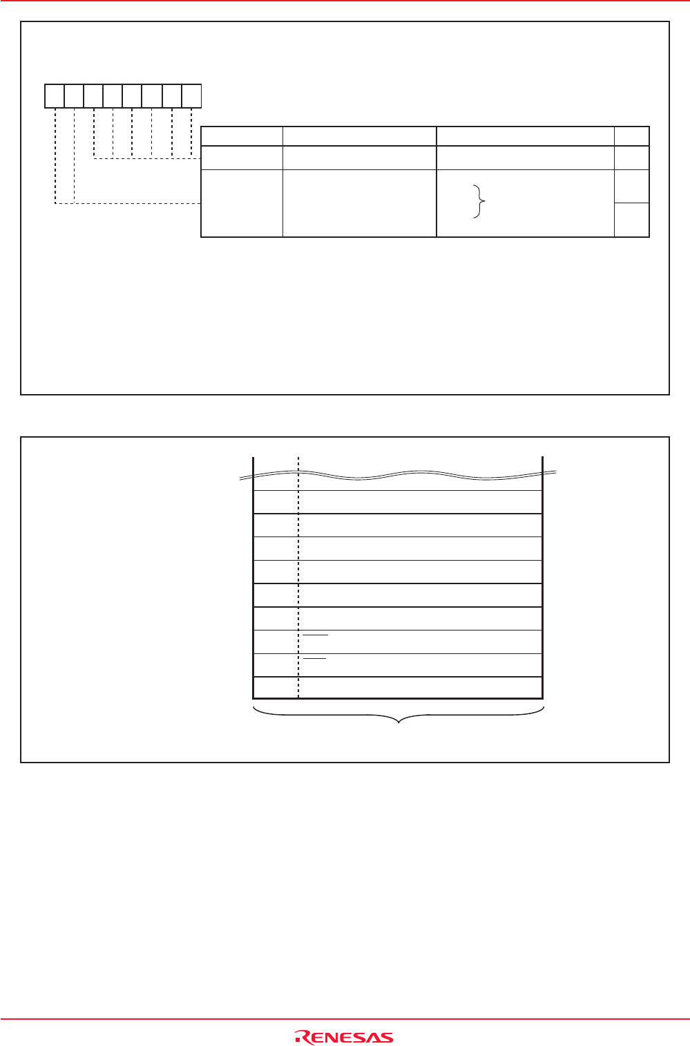
Figure 20.2 ROMCP Register
Figure 20.3 Address for ID Code Stored
ROM Code Protect Control Address
Symbol Address Value when Shipped
ROMCP 0FFFFFh FFh
(1)
b7 b6 b5 b4 b3 b2 b1 b0
1
Bit Symbol
Bit Name Function
Reserved Bit
ROM Code Protect Level 1
Set Bit
(1) (2) (3) (4)
Set to "1" RW
RW
RW
RW
-
(b5-b0)
ROMCP1
111 11
b7 b6
0 0 :
0 1 : Protect enabled
1 0 :
1 1 : Protect disabled
NOTES:
1. If a memory block that including ROMCP register is erased, the ROMCP register is set to "FFh".
2. If the ROMCP1 bit is set to other than "11b" (ROM code protect enabled), the flash memory is disabled
against reading and rewriting in parallel I/O mode.
3. When the ROMCP1 bit is set to other than "11b", set the bit 5 to bit 0 to "111111b".
If the bit 5 to bit 0 are set to other than "111111b", ROM code protect function may not become effective
even if the RPMCP1 bit is set to other than "11b".
4. When exiting ROM code protect, erase the block including the ROMCP register by CPU rewrite mode or
standard serial I/O or CAN I/O mode.
0FFFDFh to 0FFFDCh
0FFFE3h to 0FFFE0h
0FFFE7h to 0FFFE4h
0FFFEBh to 0FFFE8h
0FFFEFh to 0FFFECh
0FFFF3h to 0FFFF0h
0FFFF7h to 0FFFF4h
0FFFFBh to 0FFFF8h
0FFFFFh to 0FFFFCh
Reset vector
Oscillation stop and re-oscillation detection/Watchdog timer vector
Single step vector
Address match vector
BRK instruction vector
Overflow vector
Undefined instruction vector
NMI vector
DBC vector
ID7
ROMCP
ID6
ID5
ID4
ID3
ID2
ID1
Address
4 bytes


