


Rev.1.02 Jul 01, 2005 page 68 of 314
REJ09B0126-0102
M16C/6N Group (M16C/6NL, M16C/6NN) 9. Interrupt
Under development
This document is under development and its contents are subject to change.
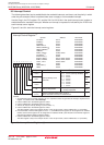
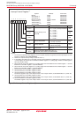
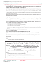
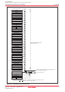
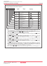
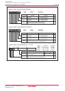
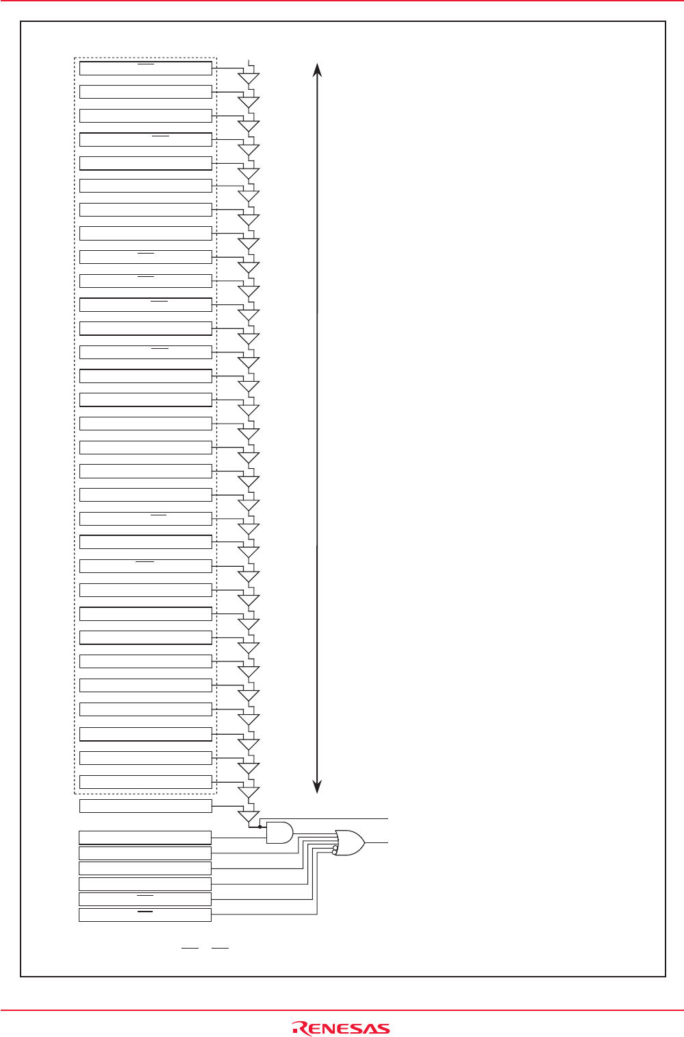
Figure 9.10 Interrupts Priority Select Circuit
Timer B2
Timer B0, SI/O6
(2)
Timer A3, INT6
(2)
Timer A1
Timer B1, INT8
(2)
Timer A4
DMA1
DMA0
SI/O3, INT4
INT1
UART2 Reception, ACK2
Level 0
(initial value)
Priority level of each interrupt
Highest
Lowest
Priority of peripheral function interrupts
(if priority levels are same)
UART1 Reception, ACK1
UART0 Reception, ACK0
Timer A2, INT7
(2)
Timer A0
INT2
INT0
INT3
Timer B5, SI/O5
(2)
Interrupt request level resolution output to clock generating circuit
(Figure 7.1 Clock Generating Circuit)
Interrupt request accepted
IPL
I Flag
DBC
NMI
SI/O4, INT5
NOTES:
1. If the PCLK6 bit in the PCLKR register is set to "1", the priority level of key input interrupt can be changed.
2. The SI/O5, SI/O6 and INT6 to INT8 registers are only in the 128-pin version.
UART1 Transmission, NACK1
UART0 Transmission, NACK0
A/D Conversion, Key Input
(1)
UART2 Bus Collision Detection
CAN0 Successful Reception
UART2 Transmission, NACK2
CAN0 Error (, Key Input)
(1)
Timer B4, UART1 Bus Collision Detection
Timer B3, UART0 Bus Collision Detection
CAN0 Successful Transmission
CAN0 Wake-up
Oscillation Stop and Re-oscillation Detection
Watchdog Timer
Address Match