


System Controller: PCI Bus Control Signals
10006757-02 PmPPC7448 User’s Manual
5-7
PCI Interface Registers
PCI0 and PCI1 contain the same set of internal registers, but are located at different offsets.
A CPU access to the MV64460 PCIx Configuration register is performed via the PCIx Config-
uration Address and Data registers. Only PCI0 is functional on the PmPPC7448.
All PCI configuration registers are located at their standard offset in the configuration
header, as defined in the PCI specification, when accessed from their corresponding PCI
bus. For example, if a master on PCI0 performs a PCI configuration cycle on PCI’s Status and
Command register, the register is located at 0x004.
The PmPPC7448 module may generate interrupts to other PCI devices by accessing door-
bell-type interrupt-generating registers or address ranges within their PCI bridges. The
module will respond to interrupts caused by another PCI device when it accesses a pro-
grammable range of local memory, as provided by the MV64460 memory controller. In
addition, it may monitor the state of the PCI bus INTA*—INTD* signals routed directly to the
memory controller’s multipurpose pins (MPP). The MV64460 contains registers that con-
trol the masking, unmasking, and priority of the PMC interrupts as inputs to the processor.
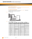
PCI BUS CONTROL SIGNALS
The following signals for the PCI interface are available on connectors P11, P12, and P13.
Refer to the PCI specification for details on using these signals. All signals are bi-directional
unless stated otherwise. A sustained tri-state line is driven high for one clock cycle before
float.
Note: The PmPPC7448 host board must adhere to the PCI Local Bus Specification (Revision 2.3) for terminating
JTAG signals.
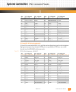
ACK64*: ACKNOWLEDGE 64-bit TRANSFER This sustained three-state signal indicates the target is
willing to transfer data using 64 bits.
AD[31:00]: ADDRESS and DATA bus (bits 0-31) These three-state signals are used for both address
and data handling. A bus transaction consists of an address phase followed by one or more
data phases.
AD[63:32]: ADDRESS and DATA bus (bits 32-63) These provide 32 additional bits. During an address
phase the upper 32-bits of a 64-bit address are transferred; otherwise these bits are
reserved. During a data phase, an additional 32-bits of data are transferred when a 64-bit
transaction has been negotiated by the assertion of REQ64* and ACK64*.
C/BE[3:0]*: BUS COMMAND and BYTE ENABLES These three-state signals have different functions
depending on the phase of a transaction. During the address phase of a transaction these
lines define the bus command. During a data phase the lines are used as byte enables.