Development Mezzanine Card: DMC Jumpers (JP1)
10006757-02 PmPPC7448 User’s Manual
10-9
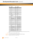
Table 10-5: DMC P4 Pin Assignments
CPLD_TCK: Test Clock Input—this is the clock input to the boundary scan test (BST) circuitry. Some
operations occur at the rising edge, while others occur at the falling edge.
CPLD_TDI: Test Data Input—this is the serial input pin for instructions as well as test and programming
data. Data is shifted in on the rising edge of TCK.
CPLD_TDO: Test Data Output—this is the serial data output pin for instructions as well as test and pro-
gramming data. Data is shifted out on the falling edge of TCK.
CPLD_TMS: Test Mode Select—this input pin provides the control signal to determine the transitions of
the TAP controller state machine. Transitions within the state machine occur at the rising
edge of TCK. Therefore, TMS must be set up before the rising edge of TCK. TMS is evaluated
on the rising edge of TCK.
DMC JUMPERS (JP1)
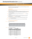
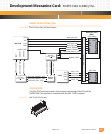
There are a total of five jumper pairs on the DMC. Pins 9 and 10 are spare jumper posts. See
Fig. 10-1 for the jumper location on the DMC.
Figure 10-7: DMC JP1 Pin Assignments
JP1: The Ethernet configuration jumper (pins 1 and 2) is not used for the PmPPC7448.
JP2: JP2 (pins 3 and 4) selects the 8-bit ROM socket as the boot device. So in order for the socket
to provide boot code, the DMC must be seated on the PmPPC7448 and the boot jumper
must be in place.
Pin: Signal: Pin: Signal:
1CPLD_TCK 2GND
3 CPLD_TDO 4 Fused 3.3 V
5CPLD_TMS 6
Not connected
7
Not connected 8 Not connected
9CPLD_TDI 10GND
SPARE
ENET
BOOT
JP3
JP4
1
2
9
10
3
4
5
6
7
8
(JP1)
(JP2)


