


EPSON Stylus Scan 2500 Revision A
Appendix Connector 143
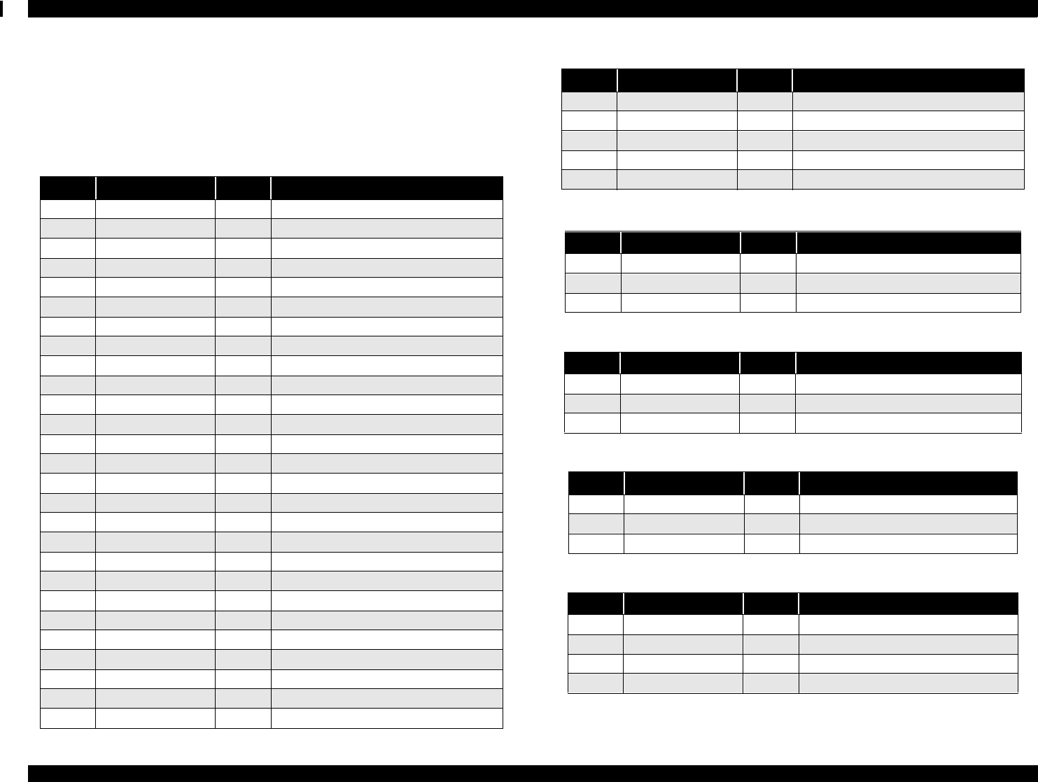
7.1.2 Connector Pin Assignment
Tables in this section provide connector pin assignment of the Stylus Scan
2500.
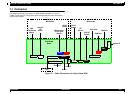
Signals of each connector on the B102 MAIN Board are listed below.
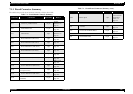
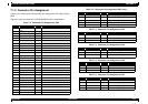
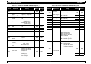
Table 7-2. Connector Pin Assignment-CN2
Pin No. Signal Name I/O Function
1 GND O Ground
2 LD0 O
3 GND O Ground
4 LD1 O
5 LED0 O LED drive signal (0)
6 LD2 O
7 LED1 O LED drive signal (1)
8 LD3 O
9 LED2 O LED drive signal (2)
10 LA0 O
11 LED3 O LED drive signal (3)
12 LCS O
13 LED4 O LED drive signal (4)
14 LWE O
15 +5V O
16 LRD O
17 +5V O
18 LCLK O
19 SW1 I Panel switch input (1)
20 SW2 I Panel switch input (2)
21 SW3 I Panel switch input (3)
22 SW4 I Panel switch input (4)
23 SW6 I Panel switch input (6)
24 SW7 I Panel switch input (7)
25 SW8 I Panel switch input (8)
26 SW9 I Panel switch input (9)
27 SW10 I Panel switch input (10)
28 SW11 I Panel switch input (11)
29 SW12 I Panel switch input (12)
30 SW5 I Panel switch input (5)
31 SW13 I Panel switch input (13)
32 SW14 I Panel switch input (14)
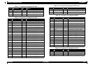
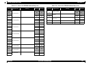
Table 7-3. Connector Pin Assignment-CN4
Pin No. Signal Name I/O Function
1 HP I Sensor detect signal
2 GND O Ground
3 HPV O Sensor power supply (+5V)
Table 7-4. Connector Pin Assignment-CN5
Pin No. Signal Name I/O Function
1 PE I Sensor detect signal
2 GND O Ground
3 PEV O Sensor power supply (+5V)
Table 7-5. Connector Pin Assignment-CN6
Pin No. Signal Name I/O Function
1 ASF I Sensor detect signal
2 GND O Ground
3 ASFV O Sensor power supply (+5V)
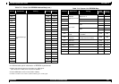
Table 7-6. Connector Pin Assignment-CN7
Pin No. Signal Name I/O Function
1 CR-A O Phase drive signal (A)
2 CR-B O Phase drive signal (B)
3 CR-/A O Phase drive signal (/A)
4 CR-/B O Phase drive signal (/B)
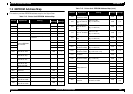
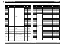
Table 7-2. Connector Pin Assignment-CN2 (cont.)
Pin No. Signal Name I/O Function