System Address Map
R
Intel
®
82845 MCH for SDR Datasheet 103
4.2.1 AGP DRAM Graphics Aperture
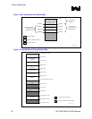
Memory-mapped, graphics data structures can reside in a Graphics Aperture to system memory.
This aperture is an address range defined by the APBASE and APSIZE registers of the MCH
device 0. The APBASE register follows the standard base address register template as defined by
the PCI Local Bus Specification, Revision 2.1. The size of the range claimed by the APBASE is
programmed via “back-end” register APSIZE (programmed by the chipset specific BIOS before
plug-and-play session is performed). APSIZE allows the BIOS software to pre-configure the
aperture size to be 4 MB, 8 MB, 16 MB, 32 MB, 64 MB, 128 MB or 256 MB. By programming
APSIZE to a specific size, the corresponding lower bits of APBASE are forced to 0 (behave as
hardwired). The default value of APSIZE forces an aperture size of 256 MB. The aperture address
range is naturally aligned.
Accesses within the aperture range are forwarded to the system memory subsystem. The MCH
translates the originally issued addresses via a translation table maintained in system memory. The
aperture range should be programmed as non-cacheable in the processor caches.
Note: Plug-and-play software configuration model does not allow overlap of different address ranges.
Therefore the AGP Graphics Aperture and AGP memory address range are independent address
ranges that may abut, but cannot overlap one another.
4.3 System Management Mode (SMM) Memory Range
The MCH supports the use of system memory as System Management RAM (SMRAM) enabling
the use of System Management Mode. The MCH supports three SMRAM options: Compatible
SMRAM (C_SMRAM), High Segment (HSEG), and Top of Memory Segment (TSEG). System
Management RAM (SMRAM) space provides a memory area that is available for the SMI
handler’s and code and data storage. This memory resource is normally hidden from the system
OS so that the processor has immediate access to this memory space upon entry to SMM. The
MCH provides three SMRAM options:
• Below 1 MB option that supports compatible SMI handlers.
• Above 1 MB option that allows new SMI handlers to execute with write-back cacheable
SMRAM.
• Optional larger write-back cacheable T_SEG area from 128 KB to 1 MB in size above 1 MB
that is reserved from the highest area in system memory. The above 1 MB solutions require
changes to compatible SMRAM handlers’ code to properly execute above 1 MB.
Note: Masters from the hub interface and AGP are not allowed to access the SMM space.


