Register Description
R
Intel
®
82845 MCH for SDR Datasheet 41
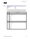
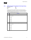
3.4.5 CKSTR—Strength Control Register (Clock Signal Group)
Memory Address Offset: 33h
Default Value: 00h
Access: R/W
Size: 8 bits
This register controls the drive strength of the I/O buffers for the Clock (CK) signal group
including both the CK and CK# signals. This group has two possible loadings depending on the
width of SDRAM devices used in each row of memory (x8 or x16). The proper strength can be
independently programmed for each configuration. The actual strength used for each signal is
determined by the DRAMWIDTH Register (offset 2Ch).
Bit Descriptions
7 Reserved.
6:4 CK x16 Strength Control. This field selects the signal drive strength.
000 = 0.75 X (default)
001 = 1.00 X
010 = 1.25 X
011 = 1.50 X
100 = 2.00 X
101 = 2.50 X
110 = 3.00 X
111 = 4.00 X
3 Reserved.
2:0 CK x8 Strength Control. This field selects the signal drive strength.
000 = 0.75 X (default)
001 = 1.00 X
010 = 1.25 X
011 = 1.50 X
100 = 2.00 X
101 = 2.50 X
110 = 3.00 X
111 = 4.00 X


