Introduction
R
Intel
®
82845 MCH for SDR Datasheet 11
1 Introduction
The Intel
®
82845 Memory Controller Hub (MCH) is designed for use with the Intel
®
Pentium
®
4
processor in the 478-pin package. The Intel
®
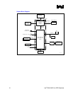
845 chipset contains two main components: the
82845 Memory Controller Hub (MCH) for the host bridge and the Intel 82801BA I/O Controller
Hub (ICH2) for the I/O subsystem. The MCH provides the processor interface, system memory
interface, AGP interface, and hub interface in an 845 chipset desktop platform.
This document describes the 82845 Memory Controller Hub (MCH) for use with SDR (Single
Data Rate) memory devices. Section 1.3 provides an overview of the 845 chipset.
1.1 Terminology and Notations
This section provides the definitions of some of the terms used in this document. Notations used
for data types and numbers are also included. In addition, Section 3.1 contains register
terminology definitions.
Table 1. General Terminology
Term Description
MCH The Memory Controller Hub component that contains the processor interface, System
Memory DRAM controller, and AGP interface. It communicates with the I/O controller
hub (ICH2) and other IO controller hubs over proprietary interconnect called the hub
interface.
ICH2 The I/O Controller Hub component that contains the primary PCI interface, LPC
interface, USB, ATA-100, AC ’97, and other I/O functions. It communicates with the
MCH over a proprietary interconnect called the hub interface.
Host This term is used synonymously with processor.
Core The internal base logic in the MCH.
System Bus Processor-to-MCH interface. The system bus runs at 400 MHz, from a 100 MHz quad-
pumped clock. It consists of source synchronous transfers for address and data, and
system bus interrupt delivery.
Hub Interface The proprietary hub interconnect that connects the MCH to the ICH2. In this document
hub interface cycles originating from or destined for the primary PCI interface on the
ICH2 are generally referred to as hub interface cycles.
Accelerated
Graphics Port
(AGP)
Refers to the AGP interface that is in the MCH. The MCH supports AGP 2.0 compliant
components only with 1.5 V signaling level. PIPE# and SBA addressing cycles and their
associated data phases are generally referred to as AGP transactions. FRAME# cycles
over the AGP bus are generally referred to as AGP/PCI transactions.
PCI_A The physical PCI bus, driven directly by the ICH2 component. It supports 5 V, 32-bit,
33 MHz PCI 2.2 compliant components. Communication between PCI_A and the MCH
occurs over the hub interface.
Note: Even though this PCI bus is referred to as PCI_A, it is not PCI Bus #0 from a
configuration standpoint.
Full Reset A full MCH reset is defined in this document when RSTIN# is asserted.


