


Functional Description
R
112 Intel
®
82845 MCH for SDR Datasheet
5.2.4 DRAM Performance Description
The overall memory performance is controlled by the DRAM Timing (DRT) Register, pipelining
depth used in the MCH, memory speed grade, and the type of SDRAM used in the system. In
addition, the exact performance in a system is also dependent on the total memory supported,
external buffering, and memory array layout. The most important contribution to overall
performance by the system memory controller is to minimize the latency required to initiate and
complete requests to memory and to support the highest possible bandwidth (full streaming, quick
turn-arounds). One measure of performance is the total flight time to complete a cache line
request. A complete discussion of performance involves the entire chipset, not just the system
memory controller.
5.2.4.1 Data Integrity (ECC)
The MCH supports single-bit Error Correcting Code (or Error Checking and Correcting) and
multiple-bit EC (Error Checking) on the system memory interface. The MCH generates an 8-bit
code word for each 64-bit QWord of memory. The MCH performs two QWord writes at a time;
thus, two 8-bit codes are sent with each write. Since the code word covers a full QWord, writes of
less than a QWord require a read-merge-write operation. Consider a DWord write to memory. In
this case, when in ECC mode, the MCH reads the QWord where the addressed DWord will be
written, merges in the new DWord, generates a code covering the new QWord, and, finally, writes
the entire QWord and code back to memory. Any correctable (single-bit) errors detected during
the initial QWord read are corrected before merging the new DWord.
The MCH also supports EC (Error Checking) data integrity mode. In this mode, the MCH
generates and stores a code for each QWord of memory. It then checks the code for reads from
memory but does not correct any errors that are found. Thus, the read performance hit associated
with ECC is not incurred.
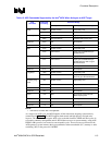
5.3 AGP Interface Overview
The MCH supports 1.5 V AGP 1x/2x/4x devices. The AGP signal buffers are 1.5 V drive/receive
(buffers are not 3.3 volt tolerant). The MCH supports 2x/4x source synchronous clocking transfers
for read and write data, and sideband addressing. The MCH also support 2x and 4x clocking for
Fast Writes initiated from the MCH (on behalf of the processor).
AGP PIPE# or SBA[7:0] transactions to system memory do not get snooped and are, therefore, not
coherent with the processor caches. AGP FRAME# transactions to system memory are snooped.
AGP PIPE# and SBA[7:0] accesses to and from the hub interface are not supported. AGP
FRAME# access from an AGP master to the hub interface are also not supported. Only the AGP
FRAME memory writes from the hub interface are supported.
5.3.1 AGP Target Operations
As an initiator, the MCH does not initiate cycles using AGP enhanced protocols. The MCH
supports AGP cycles targeting the interface to system memory only. The MCH supports
interleaved AGP PIPE# and AGP FRAME#, or AGP SBA[7:0] and AGP FRAME# transactions.