Signal Description
R
Intel
®
82845 MCH for SDR Datasheet 19
2 Signal Description
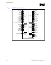
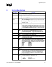
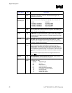
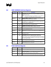
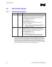
This chapter provides a detailed description of the MCH signals. The signal descriptions are
arranged in functional groups according to their associated interface (see Figure 1). The states of
all of the signals during reset are provided in the System Reset section.
The “#” symbol at the end of a signal name indicates that the active, or asserted state occurs when
the signal is at a low voltage level. When “#” is not present after the signal name the signal is
asserted when at the high voltage level.
The following notations are used to describe the signal type:
I Input pin
O Output pin
I/O Bi-directional Input/Output pin
s/t/s Sustained Three-state. This pin is driven to its inactive state prior to three-
stating.
as/t/s Active Sustained Three-state. This applies to some of the hub interface signals.
This pin is weakly driven to its last driven value.
The signal description also includes the type of buffer used for the particular signal:
AGTL+ Open Drain AGTL+ interface signal. Refer to the AGTL+ I/O Specification for
complete details. The MCH integrates AGTL+ termination resistors.
AGP AGP interface signals. These signals are compatible with AGP 2.0 1.5 V
Signaling Environment DC and AC Specifications. The buffers are not 3.3 V
tolerant.
CMOS CMOS buffers.
Ref Voltage reference signal
Note: System address and data bus signals are logically inverted signals. In other words, the actual
values are inverted of what appears on the system bus. This must be taken into account and the
addresses and data bus signals must be inverted inside the MCH. All processor control signals
follow normal convention. A “0” indicates an active level (low voltage) if the signal is followed by
“#” symbol, and a “1” indicates an active level (high voltage) if the signal has no “#” suffix.


