


Register Description
R
Intel
®
82845 MCH for SDR Datasheet 43
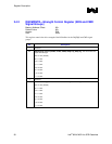
3.5 Host-Hub Interface Bridge Device Registers
(Device 0)
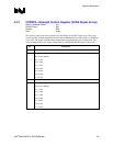
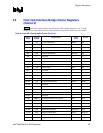
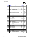
Table 8 provides the register address map for Device 0 PCI configuration space. An “s” in the
Default Value column indicates that a strap determines the power-up default value for that bit.
Table 8. Intel
®
MCH Configuration Space (Device 0)
Address
Offset
Register
Symbol
Register Name Default
Value
Access
00–01h VID Vendor Identification 8086h RO
02–03h DID Device Identification 1A30h RO
04–05h PCICMD PCI Command 0006h RO, R/W
06–07h PCISTS PCI Status 0090h RO, R/WC
08h RID Revision Identification 03h, 04h RO
09h — Reserved. — —
0Ah SUBC Sub-Class Code 00h RO
0Bh BCC Base Class Code 06h RO
0Dh MLT Master Latency Timer 00h RO
0Eh HDR Header Type 00h RO
0Fh — Reserved. — —
10–13h APBASE Aperture Base Configuration 00000008h RO, R/W
14–2Bh — Reserved. — —
2C–2Dh SVID Subsystem Vendor Identification 0000h R/WO
2E–2Fh SID Subsystem Identification 0000h R/WO
30–33h — Reserved. — —
34h CAPPTR Capabilities Pointer A0h RO
35–50h — Reserved. — —
51h AGPM AGP Miscellaneous Configuration 00h R/W
52–5Fh — Reserved. — —
60–67h DRB[0:7] DRAM Row Boundary (8 registers) 00h R/W
68–6Fh — Reserved. — —
70–73h DRA DRAM Row Attribute (4 registers) 00h R/W
73–77h — Reserved. — —
78–7Bh DRT DRAM Timing Register 00000010h R/W
7C–7Fh DRC DRAM Controller Mode 0000h R/W, RO
80–85h — Reserved. — —
86h DERRSYN DRAM Error Syndrome 00h RO