


Register Description
R
Intel
®
82845 MCH for SDR Datasheet 55
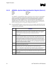
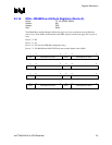
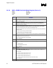
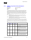
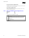
3.5.17 DRT—DRAM Timing Register (Device 0)
Offset: 78–7Bh
Default: 00000010h
Access: R/W
Size: 32 bits
Bit Description
31:19 Reserved.
18:16 DRAM Idle Timer. This field determines the number of clocks the DRAM controller will remain
in the idle state before it begins precharging all pages.
000 = infinite.
001 = 0 DRAM clocks
010 = 8 DRAM clocks
011 = 16 DRAM clocks
100 = 64 DRAM clocks
Others = Reserved
15:11 Reserved.
10:9 Activate to Precharge delay (tRAS). This bit controls the number of DRAM clocks for tRAS.
00 = 7 clocks
01 = 6 clocks
10 = 5 clocks
11 = Reserved
8:6 Reserved.
5:4 CAS# Latency (tCL). This bit controls the number of DRAM clocks between when a read
command is sampled by the SDRAMs and when the MCH samples read data from the
SDRAMs.
00 = Reserved
01 = 3 clocks
10 = 2 clocks
11 = Reserved
3 Reserved.
2 DRAM RAS# to CAS# Delay (tRCD). This bit controls the number of clocks inserted between a
row activate command and a read or write command to that row.
0 = 3 DRAM clocks
1 = 2 DRAM clocks
1 Reserved.
0 DRAM RAS# Precharge (tRP). This bit controls the number of clocks that are inserted
between a row precharge command and an activate command to the same row.
0 = 3 DRAM clocks
1 = 2 DRAM clocks