


Register Description
R
46 Intel
®
82845 MCH for SDR Datasheet
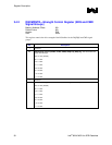
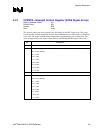
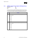
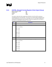
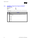
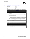
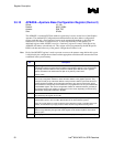
3.5.3 PCICMD—PCI Command Register (Device 0)
Address Offset: 04–05h
Default: 0006h
Access: R/W, RO
Size 16 bits
Since MCH Device 0 does not physically reside on PCI0, many of the bits are not implemented.
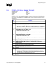
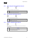
Bit Descriptions
15:10 Reserved.
9 Fast Back-to-Back—RO. Not implemented; Hardwired to 0. This bit controls whether or not the
master can do fast back-to-back write. Since device 0 is strictly a target this bit is not
implemented.
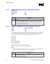
8 SERR Enable (SERRE)—R/W. This bit is a global enable bit for Device 0 SERR messaging.
The MCH does not have an SERR# signal. The MCH communicates the SERR# condition by
sending a SERR message to the ICH2.
0 = Disable. SERR message is not generated by the MCH for Device 0.
1 = Enable. The MCH is enabled to generate SERR messages over the hub interface for
specific Device 0 error conditions that are individually enabled in the ERRCMD Register. The
error status is reported in the ERRSTS and PCISTS registers.
NOTE: This bit only controls SERR message for the Device 0. Device 1 has its own SERRE
bits to control error reporting for error conditions occurring on their respective devices.
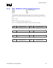
7 Address/Data Stepping—RO. Not implemented; Hardwired to 0.
6 Parity Error Enable (PERRE)—RO. Not implemented; Hardwired to 0.The PERR# signal is not
implemented by the MCH.
5 VGA Palette Snoop—RO. Not implemented; Hardwired to 0.
4 Memory Write and Invalidate Enable(MWIE)—RO. Not implemented; Hardwired to 0.
3 Special Cycle Enable(SCE)—RO. Not implemented; Hardwired to 0.
2 Bus Master Enable (BME)—RO. Hardwired to 1. The MCH is always enabled as a master on
the hub interface.
1 Memory Access Enable (MAE)—RO. Not implemented; Hardwired to 1. The MCH always
allows access to system memory.
0 I/O Access Enable (IOAE)—RO. Not implemented; Hardwired to 0.