Register Description
R
52 Intel
®
82845 MCH for SDR Datasheet
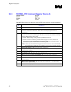
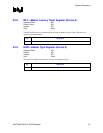
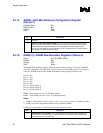
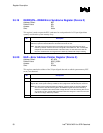
3.5.14 AGPM—AGP Miscellaneous Configuration Register
(Device 0)
Address Offset: 51h
Default Value: 00h
Access: R/W
Size: 8 bits
Bit Descriptions
7:2 Reserved.
1 Aperture Access Global Enable (APEN). This bit is used to prevent access to the graphics
aperture from any port (processor, hub interface, or AGP/PCI_B) before the aperture range is
established by the configuration software and the appropriate translation table in system
memory has been initialized. The default value is 0; thus, this field must be set after system is
fully configured to enable aperture accesses.
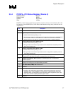
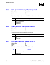
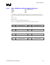
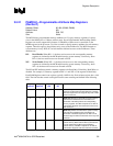
3.5.15 DRB[0:7]—DRAM Row Boundary Registers (Device 0)
Offset: 60–67h (DRB0–DRB7)
Default: 00h
Access: R/W
Size: 8 bits
The DRAM Row Boundary Register defines the upper boundary address of each pair of DRAM
rows with a granularity of 32 MB. Each row has its own single-byte DRB register. For example, a
value of 1 in DRB0 indicates that 32 MB of DRAM has been populated in the first row.
Row 0 = 60h
Row 1 = 61h
Row 2 = 62h
Row 3 = 63h
Row 4 = 64h
Row 5 = 65h (See Note 1)
Row 6 = 66h (See Note 2)
Row 7 = 67h (See Note 2)
DRB0 = Total memory in row0 (in 32 MB increments)
DRB1 = Total memory in row0 + row1 (in 32 MB increments)
Notes:
1. DRB5 = Total memory in row0 + row1 + row2 + row3 + row4 + row5 (in 32 MB increments)
2. DRB [7:6] must be programmed with the value contained in DBR5
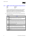
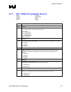
Each Row is represented by a byte. Each byte has the following format.
Bit Description
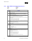
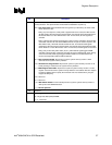
7:0 DRAM Row Boundary Address. This 8 bit value defines the upper and lower addresses for
each DRAM row. This 8-bit value is compared against a set of address lines to determine the
upper address limit of a particular row.


