LGA1155 Socket
20 Thermal/Mechanical Specifications and Design Guidelines
3.1 Board Layout
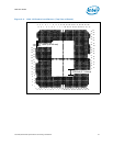
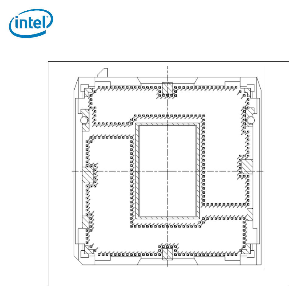
The land pattern for the LGA1155 socket is 36 mils X 36 mils (X by Y) within each of the
two L-shaped sections. Note that there is no round-off (conversion) error between
socket pitch (0.9144 mm) and board pitch (36 mil) as these values are equivalent. The
two L-sections are offset by 0.9144 mm (36 mil) in the x direction and 3.114 mm
(122.6 mil) in the y direction, see Figure 3-3. This was to achieve a common package
land to PCB land offset which ensures a single PCB layout for socket designs from the
multiple vendors.
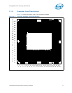
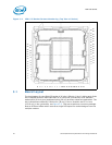
Figure 3-2. LGA1155 Socket Contact Numbering (Top View of Socket)
A C E G J L N R U W AA AC AE AG AJ AL AN AR AU AW
B D F H K M P T V Y AB AD AF AH AK AM AP AT AV AY
1
3
7
5
9
11
15
13
17
19
23
21
25
27
29
2
8
4
6
10
16
12
14
18
24
20
22
26
28
30
15
11
13
17
23
19
21
25
31
27
29
33
39
35
37
32
14
12
16
18
22
20
24
26
30
28
34
38
36
40


