


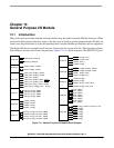

General Purpose I/O Module
MCF52211 ColdFire® Integrated Microcontroller Reference Manual, Rev. 2
Freescale Semiconductor 13-9
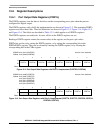
13.6.4 Port Clear Output Data Registers (CLRn)
Writing 0s to a CLRn register clears the corresponding bits in the PORTn register. Writing 1s has no effect.
Reading the CLRn register returns 0s.
The CLRn registers with a full 8-bit implementation are shown in Figure 13-17. The remaining DDRn
registers use fewer than eight bits. Their bit definitions are shown in Figure 13-18, Figure 13-19,
Figure 13-20, and Figure 13-21. The fields are described in Table 13-5, which applies to all CLRn
registers.
The CLRn registers are read/write.
Table 13-4. PORTnP/SETn Field Descriptions
Field Description
PortnPx Port nx pin data/set data bits.
1PortnPx pin state is 1 (read); writing a 1 sets the corresponding port nx bit to 1
0PortnPx pin state is 0
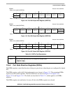
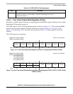
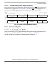
IPSBAR
Offsets:
0x10_005C (CLRDD)
0x10_0052 (CLRAN)
Access: User read/write
76543210
R
CLRn7CLRn6CLRn5CLRn4CLRn3CLRn2CLRn1CLRn0
W
Reset:00000000
Figure 13-17. Port Clear Output Data Registers with Bits 7:0 Implemented (CLRDD, CLRAN)
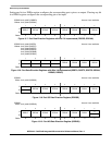
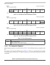
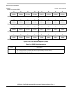
IPSBAR
Offsets:
0x10_0056 (CLRTA)
0x10_0057 (CLRTC)
0x10_0058 (CLRTD)
0x10_0059 (CLRUA)
0x10_005A (CLRUB)
0x10_005B (CLRUC)
Access: User read/write
76543210
R 0 0 0 0
CLRn3CLRn2CLRn1CLRn0
W
Reset:00000000
Figure 13-18. Port Clear Output Data Registers with Bits 3:0 Implemented (CLRTA, CLRTC, CLRTD, CLRUA,
CLRUB, CLRUC)