


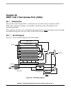

IEEE 1149.1 Test Access Port (JTAG)
MCF52211 ColdFire® Integrated Microcontroller Reference Manual, Rev. 2
Freescale Semiconductor 29-9
and held in the boundary scan update registers. EXTEST can also configure the direction of bidirectional
pins and establish high-impedance states on some pins. EXTEST asserts internal reset for the MCU system
logic to force a predictable internal state while performing external boundary scan operations.
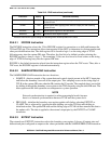
29.4.3.4 TEST_LEAKAGE Instruction
The TEST_LEAKAGE instruction forces the jtag_leakage output signal to high. It is intended to tri-state
all output pad buffers and disable all of the part’s pad input buffers except TEST and TRST. The
jtag_leakage signal is asserted at the rising edge of TCLK when the TAP controller transitions from
update-IR to run-test/idle state. After asserted, the part disables the TCLK, TMS, and TDI inputs into
JTAG and forces these JTAG inputs to logic 1. The TAP controller remains in the run-test/idle state until
the TRST input is asserted (logic 0).
29.4.3.5 ENABLE_TEST_CTRL Instruction
The ENABLE_TEST_CTRL instruction selects a 3-bit shift register (TEST_CTRL) for connection as a
shift path between the TDI and TDO pin. When the user transitions the TAP controller to the UPDATE_DR
state, the register transfers its value to a parallel hold register. It allows the control chip to test functions
independent of the JTAG TAP controller state.
29.4.3.6 HIGHZ Instruction
The HIGHZ instruction eliminates the need to backdrive the output pins during circuit-board testing.
HIGHZ turns off all output drivers, including the 2-state drivers, and selects the bypass register. HIGHZ
also asserts internal reset for the MCU system logic to force a predictable internal state.
29.4.3.7 LOCKOUT_RECOVERY Instruction
If a user inadvertently enables security on a MCU, the LOCKOUT_RECOVERY instruction allows the
disabling of security by the complete erasure of the internal flash contents including the configuration
field. This does not compromise security as the entire contents of the user’s secured code stored in flash
gets erased before security is disabled on the MCU on the next reset or power-up sequence.
The LOCKOUT_RECOVERY instruction selects a 7-bit shift register for connection as a shift path
between the TDI pin and the TDO pin. When the user transitions the TAP controller to the UPDATE-DR
state, the 7-bit shift register is loaded into the 7-bit JTAG_TFM_CLKDIV register and this value is output
to the TFM’s clock divider circuit. When the user transitions the TAP controller to the RUN-TEST/IDLE
state, the erase signal to the TFM asserts and the lockout sequence starts. The controller must remain in
that state until the erase sequence has completed. After the lockout recovery sequence has completed, the
user must reset the JTAG TAP controller and the MCU to return to normal operation.
29.4.3.8 CLAMP Instruction
The CLAMP instruction selects the bypass register and asserts internal reset while simultaneously forcing
all output pins and bidirectional pins configured as outputs to the fixed values that are preloaded and held
in the boundary scan update register. CLAMP enhances test efficiency by reducing the overall shift path