


Analog-to-Digital Converter (ADC)
MCF52211 ColdFire® Integrated Microcontroller Reference Manual, Rev. 2
Freescale Semiconductor 26-7
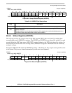
12
SYNC1
Synchronization 1 Enable bit. In parallel-scan modes when SIMULT equaling 0, setting SYNC1 allows a
conversion to be initiated by asserting a positive edge on the SYNC1 input. Any subsequent SYNC1 input
pulses that occur during the scan are ignored. In once sequential and once parallel scan modes, only the
first SYNC1 input pulse is honored. Subsequent SYNC1 input pulses are ignored until SYNC1 input is
re-armed by setting SYNC1. This can be done at any time, even during the execution of the scan. The ADC
must be in a stable power configuration prior to writing to START0 (see Section 26.5.8, “Power
Management”).
0 Scan is initiated by a write to the START1 bit only
1 Scan is initiated by a SYNC1 input pulse or a write to the START1 bit
11
EOSIE1
End of Scan Interrupt 1 Enable bit. In parallel-scan modes when SIMULT equaling 0, this bit enables an
EOSI1 interrupt to be generated upon completion of the scan. For looping scan modes, the interrupt triggers
after the completion of each iteration of the loop.
0 Interrupt disabled
1 Interrupt enabled
10–6 Reserved, should be cleared.
5
SIMULT
Simultaneous Mode bit. This bit only affects parallel scan modes.
When SIMULT equals 1, parallel scans operate in simultaneous mode. The scans in the A and B converter
operate simultaneously and always result in pairs of simultaneous conversions in the A and B converter.
START0, STOP0, SYNC0, and EOSIE0 control bits and the SYNC0 input are used to start and stop scans
in both converters simultaneously. A scan ends in both converters when either converter encounters a
disabled sample slot. When the parallel scan completes, the EOSI0 triggers if EOSIE0 is set. The CIP0
status bit indicates that a parallel scan is in process.
When SIMULT equals 0, parallel scans in the A and B converters operate independently. The B converter
has its own independent set of the above controls (START1, STOP1, SYNC1, EOSIE1, SYNC1) designed to
control its operation and report its status. Each converter’s scan continues until its sample list is exhausted
(four samples) or a disabled sample is encountered. For looping parallel scan mode, each converter starts
its next iteration as soon as the previous iteration in that converter is complete and continues until the STOP
bit for that converter is asserted.
0 Parallel scans occur independently
1 Parallel scans occur simultaneously (default)
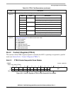
4–0
DIV
Clock Divisor Select. This field controls the divider circuit, which generates the ADC clock by dividing the
system clock by 2×DIV+1. DIV must be chosen so the ADC clock does not exceed 5.0 MHz. See Ta ble 26- 5
for a listing of ADC clock frequency based on the value of DIV for several configurations.
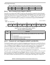
Table 26-5. ADC Clock Frequency for Various Conversion Clock Sources
DIV Divisor
ROSC Standby
400 kHz
ROSC Normal
8MHz
PLL
64 MHz
External CLK
200 kHz Sys Clock 4 MHz Sys Clock 32 MHz Sys Clock CLK/2 Sys Clock
00000 2 100 kHz 2.00 MHz
16.0 MHz CLK/4
00001 4 100 kHz 1.00 MHz 8.00 MHz CLK/8
00010 6 100 kHz 500 kHz 5.33 MHz CLK/12
00011 8 100 kHz 250 kHz 4.00 MHz CLK/16
00100 10 100 kHz 125 kHz 3.20 MHz CLK/20
——————
Table 26-4. CTRL2 Field Descriptions Under Parallel Scan Modes (continued)
Field Description