


Analog-to-Digital Converter (ADC)
MCF52211 ColdFire® Integrated Microcontroller Reference Manual, Rev. 2
Freescale Semiconductor 26-19
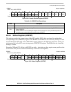
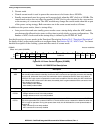
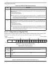
10
PSTS0
Converter A Power Status bit. This bit is asserted immediately after PD0 is set. It is deasserted PUDELAY
ADC clock cycles after PD0 is cleared if APD is 0. This bit can be read as a status bit to determine when the
ADC is ready for operation. During auto power-down mode, this bit indicates the current powered state of
converter A.
0 = ADC converter A is currently enabled
1 = ADC converter A is currently disabled
9–4
PUDELAY
Power-Up Delay. This field determines the number of ADC clock cycles provided to enable an ADC converter
(after clearing PD0 or PD1) before allowing a scan to start. It also determines the number of ADC clock
cycles of delay provided in auto power-down (APD) and auto standby (ASB) modes between when the ADC
goes from the idle to active state and when the scan is allowed to start. The default value is 13 ADC clock
cycles. Accuracy of the initial conversions in a scan is degraded if PUDELAY is too low.
Note: PUDELAY defaults to a value typically sufficient for any power mode. The latency of a scan can be
reduced by reducing PUDELAY to the lowest value for which accuracy is not degraded. Please refer
to the Device Data Sheet for further details.
3
APD
Auto Power-Down Mode bit. Auto power-down mode disables converters when they are not in use for a scan.
APD takes precedence over ASB. When a scan is started in APD mode, a delay of PUDELAY ADC clock
cycles is imposed during which the needed converter(s), if idle, are enabled. The ADC then initiates a scan
equivalent to when APD is not active. When the scan is completed, the converter(s) are disabled again.
0 Auto power-down mode is not active
1 Auto power-down mode is active
Note: If ASB or APD is asserted while a scan is in progress, that scan is unaffected and the ADC waits to
enter its low-power state until after all conversions are complete and both ADCs are idle.
Note: ASB and APD are not useful in looping modes. The continuous nature of scanning means the ADC
can never enter the low-power state.
2
PD2
Power-Down Control for Voltage Reference Circuit bit. This bit controls the power-down of the ADC’s voltage
reference circuit. This circuit is shared by both converters. When PD2 is set, the voltage reference is activated
when PD1 or PD0 are enabled. It is not usually necessary to modify this bit, because disabling
(powering-down) converter A and converter B automatically powers-down the voltage reference.
0 Manually power-up voltage reference circuit
1 Power-down voltage reference circuit is controlled by PD0 and PD1 (default)
Table 26-18. POWER Field Descriptions (continued)
Field Description