


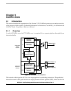

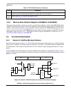
ColdFire Core
MCF52211 ColdFire® Integrated Microcontroller Reference Manual, Rev. 2
3-8 Freescale Semiconductor
3.3 Functional Description
3.3.1 Version 2 ColdFire Microarchitecture
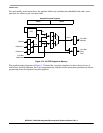
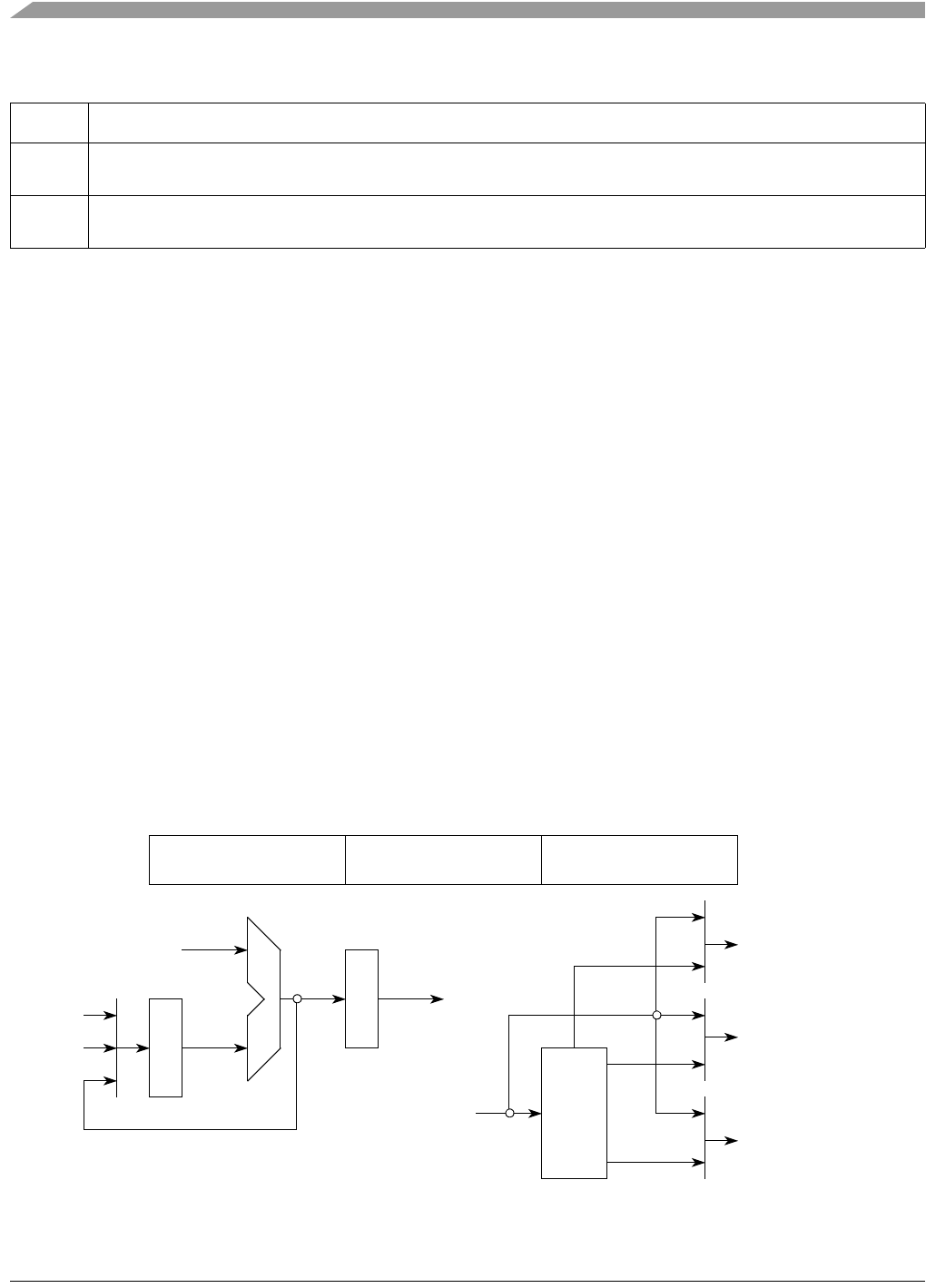
From the block diagram in Figure 3-1, the non-Harvard architecture of the processor is readily apparent.
The processor interfaces to the local memory subsystem via a single 32-bit address and two unidirectional
32-bit data buses. This structure minimizes the core size without compromising performance to a large
degree.
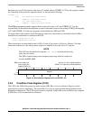
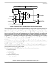
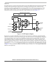
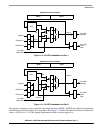
A more detailed view of the hardware structure within the two pipelines is presented in Figure 3-9 and
Figure 3-10 below. In these diagrams, the internal structure of the instruction fetch and operand execution
pipelines is shown:
Figure 3-9. Version 2 ColdFire Processor Instruction Fetch Pipeline Diagram
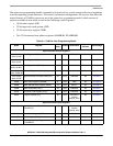
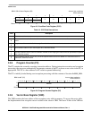
10–8
I
Interrupt level mask. Defines current interrupt level. Interrupt requests are inhibited for all priority levels less than or
equal to current level, except edge-sensitive level 7 requests, which cannot be masked.
7–0
CCR
Refer to Section 3.2.4, “Condition Code Register (CCR)”.
Table 3-3. SR Field Descriptions (continued)
Field Description
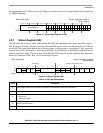
3.2.8 Memory Base Address Registers (RAMBAR, FLASHBAR)
The memory base address register sare used to specify the base address of the internal SRAM and flash
modules and indicate the types of references mapped to each. Each base address register includes a base
address, write-protect bit, address space mask bits, and an enable bit. FLASHBAR determines the base
address of the on-chip flash, and RAMBAR determines the base address of the on-chip RAM. For more
information, refer to Section 5.2.1, “SRAM Base Address Register (RAMBAR)” and Section 18.3.2,
“Flash Base Address Register (FLASHBAR)”.
IAG IC IB
Core Bus
Address
Core Bus
Read Data
Opword
Extension 1
Extension 2
FIFO
IB
+4