


LSI Specification
MB86617A
Rev.1.0 Fujitsu VLSI
16
5.4. MPU Interface
This section explains the pin function of MPU interface.
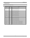
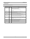
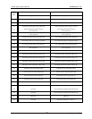
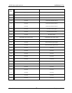
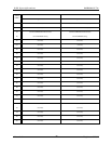
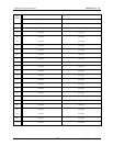
Signal Name I/O Function
A7 – 1 I
Address input pin for selecting internal register
Available only when selecting non-multi mode
When selecting multiplex mode, set this signal in fixed ‘L’
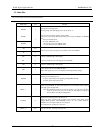
D15 - 8,0
AD7 – 1
I/O
Data I/O pin
Corresponding to address input signal when selecting multiplex mode
XCS I Chip enable input pin for this device
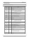
XRD(R/W) I
80 system mode: read out strobe input pin for this device
68 system mode: input pin for controlling read out/write for this device
XWR(XDS) I
80 system mode: strobe input pin for writing into this device
68 system mode: input pin of XDS signal to be output with data bus in available
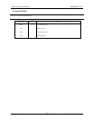
ALE I
Input pin of ALE signal to be output with its address in available when selecting
multiplex mode
When selecting non-multiplex mode, set this signal in fixed ‘L’
DREQ O Output pin of DMA transfer requiring signal for DMAC
XDACK I Input pin of DMA allowance signal from DMAC
XINT O Output pin for interruption request