


9-3
INTERFACING WITH EXTERNAL MEMORY
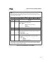
CCR1
no direct access
†
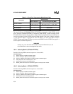
The chip configuration 1 (CCR1) register enables the watchdog timer and selects the bus timing
mode. Two of its bits combine with three bits of CCR0 to control wait states and bus width. Another bit
controls whether CCR2 is loaded.
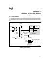
7 0
MSEL1 MSEL0 0 1 WDE BW1 IRC2 LDCCB2
Bit
Number
Bit
Mnemonic
Function
7:6 MSEL1:0 External Access Timing Mode Select
These bits control the bus-timing modes.
MSEL1 MSEL0
0 0 standard mode plus one wait state
0 1 reserved
1 0 reserved
1 1 standard mode
5 0 To guarantee proper operation, write zero to this bit.
4 1 To guarantee proper operation, write one to this bit.
3 WDE Watchdog Timer Enable
Selects whether the watchdog timer is always enabled or enabled the
first time it is cleared.
0 = always enabled
1 = enabled first time it is cleared
2 BW1 Buswidth Control
This bit, along with the BW0 bit (CCR0.1), selects the bus width.
BW1 BW0
0 0 illegal
0 1 16-bit only
1 0 8-bit only
1 1 BUSWIDTH pin controlled
†
The CCRs are loaded with the contents of the chip configuration bytes (CCBs) after reset, unless the
microcontroller is entering programming modes, in which case the programming chip configuration
bytes (PCCBs) are used. The CCBs reside in internal nonvolatile memory at addresses FF2018H
(CCB0), FF201AH (CCB1), and FF201CH (CCB2).
Figure 9-2. Chip Configuration 1 (CCR1) Register