


87C196CB Supplement
A-6
BREQ# O Bus Request
This active-low output signal is asserted during a hold cycle when the bus
controller has a pending external memory cycle.
The device can assert BREQ# at the same time as or after it asserts HLDA#.
Once it is asserted, BREQ# remains asserted until HOLD# is removed.
You must enable the bus-hold protocol before using this signal.
BREQ# is multiplexed with P2.3.
BUSWIDTH I Bus Width
The chip configuration register bits, CCR0.1 and CCR1.2, along with the
BUSWIDTH pin, control the data bus width. When both CCR bits are set, the
BUSWIDTH signal selects the external data bus width. When only one CCR bit
is set, the bus width is fixed at either 16 or 8 bits, and the BUSWIDTH signal
has no effect.
CCR0.1 CCR1.2 BUSWIDTH
0 1 N/A fixed 8-bit data bus
1 0 N/A fixed 16-bit data bus
1 1 high 16-bit data bus
1 1 low 8-bit data bus
BUSWIDTH is multiplexed with P5.7.
CLKOUT O Clock Output
Output of the internal clock generator. The CLKOUT frequency is ½ the
operating frequency (f). CLKOUT has a 50% duty cycle.
CLKOUT is multiplexed with P2.7 and PACT#.
COMP1:0 O Event Processor Array (EPA) Compare Pins
These signals are the output of the EPA compare-only channels. These pins
are multiplexed with other signals and may be configured as standard I/O.
COMP1:0 are multiplexed as follows: COMP0/P6.0/EPA8 and
COMP1/P6.1/EPA9.
CPVER O Cumulative Program Verification
During slave programming, a high signal indicates that all locations
programmed correctly, while a low signal indicates that an error occurred during
one of the programming operations.
CPVER is multiplexed with P2.6 and HLDA#.
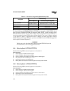
Table A-3. Signal Descriptions (Continued)
Name Type Description