


2-3
ARCHITECTURAL OVERVIEW
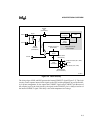
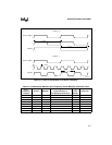
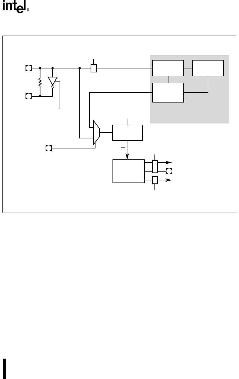
Figure 2-2. Clock Circuitry
The rising edges of PH1 and PH2 generate the internal CLKOUT signal (Figure 2-3). The clock
circuitry routes separate internal clock signals to the CPU and the peripherals to provide flexibil-
ity in power management. It also outputs the CLKOUT signal on the CLKOUT pin. Because of
the complex logic in the clock circuitry, the signal on the CLKOUT pin is a delayed version of
the internal CLKOUT signal. This delay varies with temperature and voltage.
A3168-01
Clock
Generators
CPU Clocks (PH1, PH2)
Divide-by-two
Circuit
PLLEN
Phase-locked Loop
Clock Multiplier
Phase
Comparator
Filter
Phase-
locked
Oscillator
Disable
PLL
(Powerdown)
Peripheral Clocks (PH1, PH2)
CLKOUT
Disable Clocks
(Powerdown)
Disable Clocks
(Idle, Powerdown)
XTAL1
XTAL2
F
XTAL1
Disable
Oscillator
(Powerdown)
Disable Clock Input
(Powerdown)
f
F
XTAL1
4F
XTAL1
f
2