


87C196CB Supplement
A-10
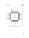
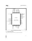
P6.7:0 I/O Port 6
This is a standard 8-bit bidirectional port.
Port 6 is multiplexed as follows: P6.0/EPA8/COMP0, P6.1/EPA9/COMP1,
P6.2/T1CLK, P6.3/T1DIR, P6.4/SC0, P6.5/SD0, P6.6/SC1, and P6.7/SD1.
PACT# O Programming Active
During auto programming or ROM-dump, a low signal indicates that
programming or dumping is in progress, while a high signal indicates that the
operation is complete.
PACT# is multiplexed with P2.7 and CLKOUT.
PALE# I Programming ALE
During slave programming, a falling edge causes the device to read a
command and address from the PBUS.
PALE# is multiplexed with P2.1 and RXD.
PBUS15:0 I/O Address/Command/Data Bus
During slave programming, ports 3 and 4 serve as a bidirectional port with
open-drain outputs to pass commands, addresses, and data to or from the
device. Slave programming requires external pull-up resistors.
During auto programming and ROM-dump, ports 3 and 4 serve as a regular
system bus to access external memory. P4.6 and P4.7 are left unconnected;
P1.1 and P1.2 serve as the upper address lines.
Slave programming:
PBUS.7:0 are multiplexed with AD7:0, SLP7:0, and P3.7:0.
PBUS.15:8 are multiplexed with AD15:8 and P4.7:0.
Auto programming:
PBUS.7:0 are multiplexed with AD7:0, SLP7:0, and P3.7:0.
PBUS.13:8 are multiplexed with AD13:8 and P4.5:0; PBUS15:14 are
multiplexed with P1.2:1.
PMODE.3:0 I Programming Mode Select
The value on the PMODE pins determines the programming mode:
0H = serial port programming
5H = slave programming
6H = ROM-dump
CH = auto programming
PMODE is sampled after a device reset and must be static while the part is
operating.
PMODE.3:0 are multiplexed with P0.7:4 and ACH7:4.
PLLEN I Phase-locked Loop Enable
This input pin enables and disables the on-chip clock multiplier feature.
0 = standard mode; internal frequency is equal to F
XTAL1.
1 = quadruple mode; internal frequency is equal to 4F
XTAL1.
Table A-3. Signal Descriptions (Continued)
Name Type Description