


87C196CB SUPPLEMENT
9-4
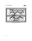
1 IRC2 Ready Control
This bit, along with IRC0 (CCR0.4) and IRC1 (CCR0.5), limits the number
of wait states that can be inserted while the READY pin is held low. Wait
states are inserted into the bus cycle either until the READY pin is pulled
high or until this internal number is reached.
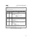
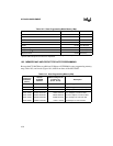
IRC2 IRC1 IRC0
0 0 0 zero wait states
0 X 1 illegal
1 1 X illegal
1 0 0 one wait state
1 0 1 two wait states
1 1 0 three wait states
1 1 1 READY pin controlled
If you choose the READY pin controlled option, you must keep P5.6
configured as a special-function input, and add external hardware to
count wait states and release READY within a specified time.
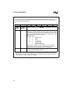
0 LDCCB2 Load CCB2
Setting this bit causes CCB2 to be read.
CCR1 (Continued)
no direct access
†
The chip configuration 1 (CCR1) register enables the watchdog timer and selects the bus timing
mode. Two of its bits combine with three bits of CCR0 to control wait states and bus width. Another bit
controls whether CCR2 is loaded.
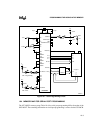
7 0
MSEL1 MSEL0 0 1 WDE BW1 IRC2 LDCCB2
Bit
Number
Bit
Mnemonic
Function
†
The CCRs are loaded with the contents of the chip configuration bytes (CCBs) after reset, unless the
microcontroller is entering programming modes, in which case the programming chip configuration
bytes (PCCBs) are used. The CCBs reside in internal nonvolatile memory at addresses FF2018H
(CCB0), FF201AH (CCB1), and FF201CH (CCB2).
Figure 9-2. Chip Configuration 1 (CCR1) Register (Continued)