


7-5
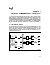
CAN SERIAL COMMUNICATIONS CONTROLLER
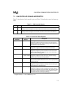
7.3.1 Address Map
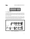
The CAN controller has 256 bytes of RAM, containing 15 message objects and control and status
registers at fixed addresses. Each message object occupies 15 consecutive bytes beginning at a
base address that is a multiple of 16 bytes. The byte above each message object is reserved (indi-
cated by a dash (—) character) or occupied by a control register. The lowest 16 bytes of RAM
contain the remaining control and status registers (Table 7-3). This 256-byte section of memory
can be windowed for register-direct access.
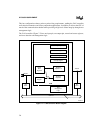
7.3.2 Message Objects
The CAN controller includes 15 message objects, each of which occupies 15 bytes of RAM (Ta-
ble 7-4). Message objects 1–14 can be configured to either transmit or receive messages, while
message object 15 can only receive messages. Message objects 1–14 have only a single buffer,
so if a second message is received before the CPU reads the first, the first message is overwritten.
Message object 15 has two alternating buffers, so it can receive a second message while the first
is being processed. However, if a third message is received while the CPU is reading the first, the
second message is overwritten.
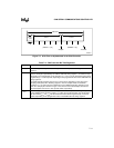
Table 7-3. CAN Controller Address Map
Hex Address Description Hex Address Description
1EFF — 1E6F —
1EF0–1EFE Message Object 15 1E60–1E6E Message Object 6
1EEF — 1E5F Interrupt Register
1EE0–1EEE Message Object 14 1E50–1E5E Message Object 5
1EDF — 1E4F Bit Timing Register 1
†
1ED0–1EDE Message Object 13 1E40–1E4E Message Object 4
1ECF — 1E3F Bit Timing Register 0
†
1EC0–1ECE Message Object 12 1E30–1E3E Message Object 3
1EBF — 1E2F —
1EB0–1EBE Message Object 11 1E20–1E2E Message Object 2
1EAF — 1E1F —
1EA0–1EAE Message Object 10 1E10–1E1E Message Object 1
1E9F — 1E0C–1E0F Message 15 Mask Register
1E90–1E9E Message Object 9 1E08–1E0B Extended Global Mask Register
1E8F — 1E06–1E07 Standard Global Mask Register
1E80–1E8E Message Object 8 1E02–1E05 —
1E7F — 1E01 Status Register
1E70–1E7E Message Object 7 1E00 Control Register
†
†
The control register’s CCE bit must be set to enable write access to the bit timing registers.