


A-1
APPENDIX A
SIGNAL DESCRIPTIONS
A.1 FUNCTIONAL GROUPINGS OF SIGNALS
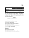
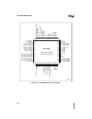
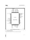
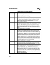
Table A-1 lists the signals for the 87C196CB, grouped by function. A diagram of each package
that is currently available shows the pin location of each signal.
NOTE
As new packages are supported, they will be added to the datasheets first. If
your package type is not shown in this appendix, refer to the latest datasheet to
find the pin locations.
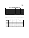
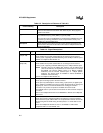
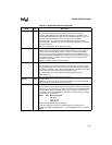
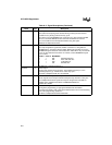
Table A-1. 87C196CB Signals Arranged by Functional Categories
Input/Output Processor Control Bus Control & Status
EPORT.7:0 (100-pin CB) EA# ALE/ADV#
EPORT.3:0 (84-pin CB) EXTINT BHE#/WRH#
P0.7:0/ACH7:0 NMI BREQ#
P1.0/EPA0/T2CLK ONCE# BUSWIDTH
P1.1/EPA1 RESET# CLKOUT
P1.2/EPA2/T2DIR SLPINT
†
HOLD#
P1.7:3/EPA7:3 XTAL1 HLDA#
P2.0/TXD XTAL2 INST
P2.1/RXD PLLEN INTOUT#
P2.7:2 Address & Data READY
P3.7:0 A23:16 (100-pin CB) RD#
P4.7:0 A19:16 (84-pin CB) SLPALE
†
P5.7:0 AD15:0 SLPCS#
†
P6.0/EPA8/COMP0 SLP7:0
†
SLPWR#
†
P6.1/EPA9/COMP1 Programming Control SLPRD#
†
P6.2/T1CLK AINC# Power & Ground
P6.3/T1DIR CPVER ANGND
P6.4/SC0 PACT# V
CC
P6.5/SD0 PALE# V
PP
P6.6/SC1 PBUS15:0 V
REF
P6.7/SD1 PMODE.3:0 V
SS,
V
SS
1
RXCAN PROG#
TXCAN PVER
†
Slave port signal