


7-3
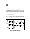
CAN SERIAL COMMUNICATIONS CONTROLLER
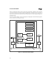
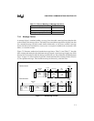
7.2 CAN CONTROLLER SIGNALS AND REGISTERS
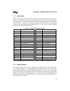
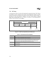
Table 7-1 describes the CAN controller’s pins, and Table 7-2 describes the control and status reg-
isters.
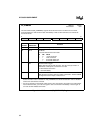
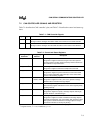
Table 7-1. CAN Controller Signals
Signal Type Description
RXCAN I Receive
This signal carries messages from other nodes on the CAN bus to the CAN controller.
TXCAN O Transmit
This signal carries messages from the CAN controller to other nodes on the CAN bus.
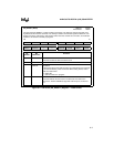
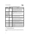
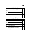
Table 7-2. Control and Status Registers
Register
Mnemonic
††
Register
Address
††
Description
CAN_BTIME0
†
1E3FH Bit Timing 0
Program this register to define the length of one time quantum
and the maximum number of time quanta by which a bit time can
be modified for resynchronization.
CAN_BTIME1
†
1E4FH Bit Timing 1
Program this register to define the sample time and mode.
CAN_CON
†
1E00H Control
Program this register to prevent transfers to and from the CAN
bus, to enable and disable CAN interrupts, and to control write
access to the bit timing registers.
CAN_EGMSK 1E08H, 1E09H,
1E0AH, 1E0BH
Extended Global Mask
Program this register to mask (“don’t care”) specific message
identifier bits for extended message objects.
CAN_INT 1E5FH CAN Interrupt Pending
This read-only register indicates the source of the highest-priority
pending interrupt.
CAN_MSG
x
CFG 1E
y
6H Message Object
x
Configuration
Program this register to specify a message object’s data length,
transfer direction, and identifier type.
CAN_MSG
x
CON0 1E
y
0H Message Object
x
Control 0
Program this register to enable or disable the message object’s
successful transmission (TX) and reception (RX) interrupts. Read
this register to determine whether a message object is ready to
transmit and whether an interrupt is pending.
†
The CCE bit in CAN_CON must be set to enable write access to the bit timing registers.
††
In register names,
x
= 1–15; in addresses,
y
= 1–F.