


87C196CB SUPPLEMENT
2-2
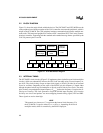
2.2 BLOCK DIAGRAM
Figure 2-1 shows the major blocks within the device. The 8XC196NT and 87C196CB have the
same peripheral set with the exception of the CAN (controller area network) peripheral, which is
unique to the 87C196CB. The CAN peripheral manages communications between multiple net-
work nodes. This integrated peripheral is similar to Intel’s standalone 82527 CAN serial commu-
nications controller, supporting both the standard and extended message frames specified by the
CAN 2.0 protocol parts A and B.
Figure 2-1. 87C196CB Block Diagram
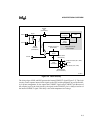
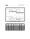
2.3 INTERNAL TIMING
The 87C196CB’s clock circuitry (Figure 2-2) implements phase-locked loop and clock multiplier
circuitry, which can substantially increase the CPU clock rate while using a lower-frequency in-
put clock. The clock circuitry accepts an input clock signal on XTAL1 provided by an external
crystal or oscillator. Depending on the value of the PLLEN pin, this frequency is routed either
through the phase-locked loop and multiplier or directly to the divide-by-two circuit. The multi-
plier circuitry can quadruple the input frequency (F
XTAL1
) before the frequency (f) reaches the di-
vide-by-two circuitry. The clock generators accept the divided input frequency (f/2) from the
divide-by-two circuit and produce two nonoverlapping internal timing signals, PH1 and PH2.
These signals are active when high.
NOTE
This manual uses lowercase “f” to represent the internal clock frequency. For
the 87C196CB, f is equal to either F
XTAL1
or 4F
XTAL1
, depending on the clock
multiplier mode, which is controlled by the PLLEN input pin.
A3179-01
OTPROM
Core
Code/Data
RAM
Clock and
Power Mgmt.
PTS
SSIO
EPAI/O
A/DSIO
Interrupt
Controller
WDT
Slave
Port
CAN