


A-9
SIGNAL DESCRIPTIONS
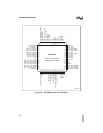
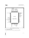
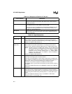
P0.7:0 I Port 0
This is a high-impedance, input-only port. Port 0 pins should not be left floating.
These pins may individually be used as analog inputs (ACH
x
) or digital inputs
(P0.
x
). While it is possible for the pins to function simultaneously as analog and
digital inputs, this is not recommended because reading port 0 while a
conversion is in process can produce unreliable conversion results.
ANGND and V
REF
must be connected for port 0 to function.
P0.7:4 are multiplexed with ACH7:4 and PMODE.3:0. P0.3:0 are multiplexed
with ACH3:0.
P1.7:0 I/O Port 1
This is a standard, bidirectional port that is multiplexed with individually
selectable special-function signals.
Port 1 is multiplexed as follows: P1.0/EPA0, P1.1/EPA1, P1.2/EPA2,
P1.3/EPA3, P1.4/T1CLK, P1.5/T1DIR, P1.6/T2CLK, and P1.7/T2DIR.
P2.7:0 I/O Port 2
This is a standard bidirectional port that is multiplexed with individually
selectable special-function signals.
P2.6 is multiplexed with the ONCE# function. If this pin is held low during reset,
the device will enter ONCE mode, so exercise caution if you use this pin for
input. If you choose to configure this pin as an input, always hold it high during
reset and ensure that your system meets the V
IH
specification (see datasheet)
to prevent inadvertent entry into a test mode.
Port 2 is multiplexed as follows: P2.0/TXD/PVER, P2.1/RXD/PALE#,
P2.2/EXTINT/PROG#, P2.3/BREQ#, P2.4/INTOUT#/AINC#, P2.5/HOLD#,
P2.6/HLDA#/ONCE#/CPVER, P2.7/CLKOUT/PACT#.
P3.7:0 I/O Port 3
This is an 8-bit, bidirectional, memory-mapped I/O port with open-drain outputs.
The pins are shared with the multiplexed address/data bus, which has comple-
mentary drivers.
P3.7:0 are multiplexed with AD7:0, SLP7:0, and PBUS.7:0.
P4.7:0 I/O Port 4
This is an 8-bit, bidirectional, memory-mapped I/O port with open-drain outputs.
The pins are shared with the multiplexed address/data bus, which has comple-
mentary drivers.
P4.7:0 are multiplexed with AD15:8 and PBUS15:8.
P5.7:0 I/O Port 5
This is an 8-bit, bidirectional, memory-mapped I/O port.
P5.4 is multiplexed with a special test-mode-entry function. If this pin is held low
during reset, the device will enter a reserved test mode, so exercise caution if
you use this pin for input. If you choose to configure this pin as an input, always
hold it high during reset and ensure that your system meets the V
IH
specification
(see datasheet) to prevent inadvertent entry into a test mode.
Port 5 is multiplexed as follows: P5.0/ALE/ADV#/SLPALE, P5.1/INST/SLPCS#,
P5.2/WR#/WRL#/SLPWR#, P5.3/RD#/SLPRD#, /SLPINT, P5.5/BHE#/WRH#,
P5.6/READY, and P5.7/BUSWIDTH.
Table A-3. Signal Descriptions (Continued)
Name Type Description