


10-4
87C196CB SUPPLEMENT
The lower 24 Kbytes of OTPROM (FF2000–FF7FFFH) are remapped to A000–FFFFH, and the
upper 32 Kbytes (FF8000–FFFFFFH) are mapped to 8000–FFFFH. A bank switching mecha-
nism differentiates between the two address ranges. The most-significant bit of an otherwise re-
served byte register (location 1FF9H) selects the bank. Bank 0 is the lower 24 Kbytes, and bank
1 is the upper 32 Kbytes. To program the lower 24 Kbytes, you must write 00H to location
1FF9H. To program the upper 32 Kbytes, you must write 80H to location 1FF9H. (See page 10-4
for the required command sequences.)
WARNING
Writing any value other than 00H or 80H to location 1FF9H will cause the
microcontroller to enter an unsupported test mode.
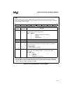
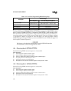
10.4.1 Selecting Bank 0 (FF2000–FF7FFFH)
Send the following RISM command sequence to select bank 0.
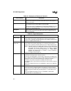
Code Description
1F DATA. High byte of address to DATA register.
F9 DATA. Low byte of address to DATA register.
0A DATA_TO_ADDR. Move address from DATA register to ADDR register.
00 SET_DLE_FLAG. The next data byte is <1FH.
00 DATA. Data to clear the most-significant bit.
07 WRITE_BYTE. Move data from the DATA register to memory location 1FF9H.
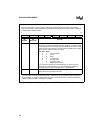
10.4.2 Selecting Bank 1 (FF8000–FFFFFFH)
Send the following RISM command sequence to select bank 1.
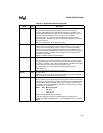
Code Description
1F DATA. High byte of address to DATA register.
F9 DATA. Low byte of address to DATA register.
0A DATA_TO_ADDR. Move address from DATA register to ADDR register.
80 DATA. Data to set the most-significant bit.
07 WRITE_BYTE. Move data from the DATA register to memory location 1FF9H.
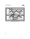
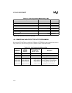
Table 10-4. Serial Port Programming Mode Memory Map
Description
Address Range
Normal Operation Serial Port Programming Mode
Internal OTPROM
FF2000–FF7FFFH
FF8000–FFFFFFH
A000–FFFFH (bank 0; 1FF9H = 00H)
8000–FFFFH (bank 1; 1FF9H = 80H)
External memory — 4000–7FFFH
Do not address — 2400–3FFFH
Test ROM and RISM — 2000–23FFH