


7-15
CAN SERIAL COMMUNICATIONS CONTROLLER
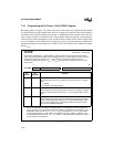
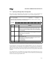
7.4.2 Programming the Bit Timing 0 (CAN_BTIME0) Register
Bit timing register 0 (Figure 7-7) defines the length of one time quantum and the maximum
amount by which the sample point can be moved (t
TSEG1
or t
TSEG2
can be shortened and the other
lengthened) to compensate for resynchronization.
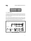
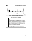
CAN_BTIME0
†
(87C196CB)
Address:
Reset State:
1E3FH
Unchanged
Program the CAN bit timing 0 (CAN_BTIME0) register to define the length of one time quantum and
the maximum number of time quanta by which a bit time can be modified for resynchronization.
7 0
87C196CB
SJW1 SJW0 BRP5 BRP4 BRP3 BRP2 BRP1 BRP0
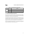
Bit
Number
Bit
Mnemonic
Function
7:6 SJW1:0 Synchronization Jump Width
This field defines the maximum number of time quanta by which a resyn-
chronization can modify t
TSEG1
and t
TSEG2
. Valid programmed values are 0–
3. The hardware adds 1 to the programmed value, so a “1” value causes
the CAN peripheral to add or subtract 2 time quanta, for example. This
adjustment has no effect on the total bit time; if t
TSEG1
is increased by 2 tq,
t
TSEG2
is decreased by 2 tq, and vice versa.
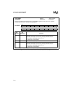
5:0 BRP5:0 Baud-rate Prescaler
This field defines the length of one time quantum (tq), using the following
formula, where t
XTAL1
is the input clock period on XTAL1. Valid programmed
values are 0–63.
For example, at 20 MHz operation, the system clock period is 50 ns.
Writing 3 to BRP achieves a time quanta of 400 ns; writing 1 to BRP
achieves a time quanta of 200 ns.
†
The CCE bit (CAN_CON.6) must be set to enable write access to this register.
Figure 7-7. CAN Bit Timing 0 (CAN_BTIME0) Register
tq 2t
XTAL1
BRP 1+()×=
tq 2 50×()31+()× 400 ns==
tq 2 50×()11+()× 200 ns==