


10-2
87C196CB SUPPLEMENT
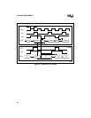
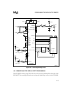
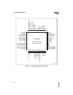
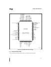
10.3 MEMORY MAP AND CIRCUIT FOR AUTO PROGRAMMING
Because the 87C196CB has an additional 24 Kbytes of OTPROM, its auto programming memory
map (Table 10-3) and circuit (Figure 10-1) differ from those of the 8XC196NT.
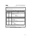
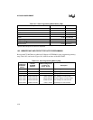
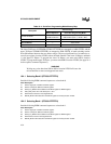
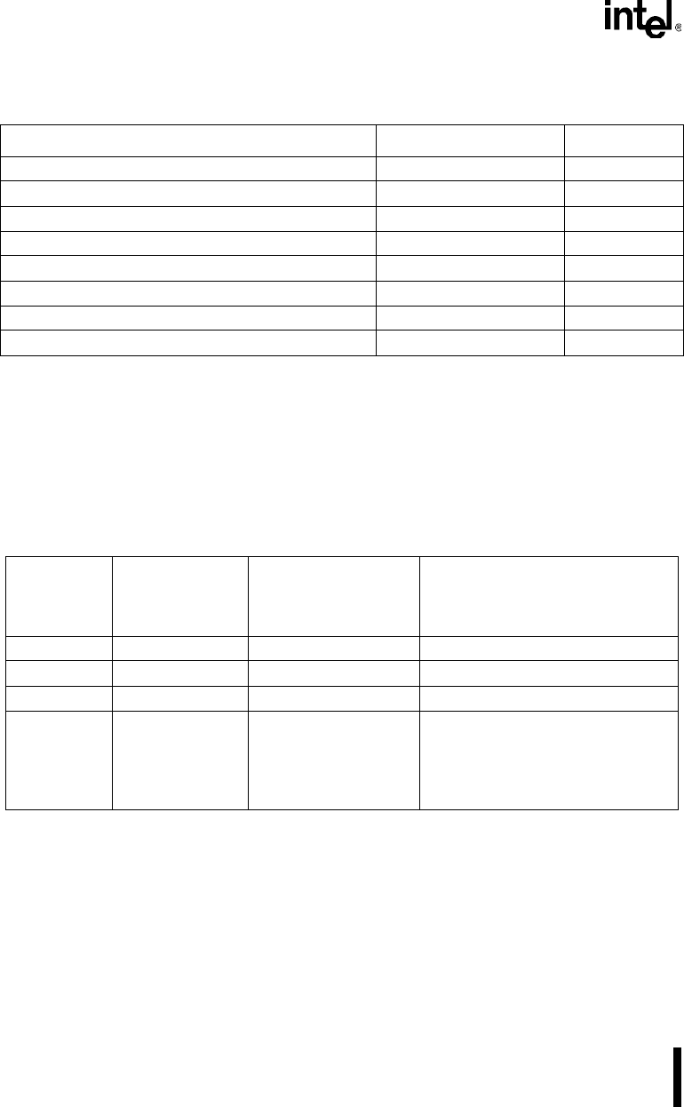
Table 10-2. Slave Programming Mode Memory Map
Description Address Comments
OTPROM FF2000–FFFFFFH OTPROM Cells
OFD 0778H OTPROM Cell
DED
†
0758H UPROM Cell
DEI
†
0718H UPROM Cell
PCCB 0218H Test EPROM
Programming V
CC
0072H Read Only
Programming V
PP
0073H Read Only
Signature word 0070H Read Only
†
These bits program the UPROM cells. Once these bits are programmed, they cannot be erased, and
dynamic failure analysis of the device is impossible.
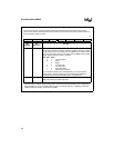
Table 10-3. Auto Programming Memory Map
Address
Output from
87C196CB
(A15:0)
Internal
OTPROM
Address
Address Using Circuit
in Figure 10-1
(P1.3:1, A13:0)
Description
4014H N/A 00014H Programming pulse width (PPW) LSB.
4015H N/A 00015H Programming pulse width (PPW) MSB.
4020–402FH FF2020–FF202FH 00020–0002FH Security key for verification.
4000–7FFFH FF2000–FF5FFFH 04000–07FFFH First 16 Kbytes of code and data.
4000–7FFFH FF6000–FF9FFFH 08000–0BFFFH Second 16 Kbytes of code and data.
4000–7FFFH FFA000–FFDFFFH 0C000–0FFFFH Third 16 Kbytes of code and data.
4000–5FFFH FFE000–FFFFFFH 10000–11FFFH Last 8 Kbytes of code and data.