


87C196CB Supplement
A-4
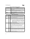
Table A-2. Description of Columns of Table A-3
Column Heading
Description
Name Lists the signals, arranged alphabetically. Many pins have two functions, so
there are more entries in this column than there are pins. Every signal is
listed in this column.
Type Identifies the pin function listed in the
Name
column as an input (I), output
(O), bidirectional (I/O), power (PWR), or ground (GND).
Note that all inputs except RESET# are
sampled inputs
. RESET# is a level-
sensitive input. During powerdown mode, the powerdown circuitry uses
EXTINT as a level-sensitive input.
Description Briefly describes the function of the pin for the specific signal listed in the
Name
column. Also lists the alternate fuction that are multiplexed with the
signal (if applicable).
Table A-3. Signal Descriptions
Name Type Description
A23:16
(100-pin CB)
I/O Address Lines 16–23
These address lines provide address bits 20–23 during the entire external
memory cycle, supporting extended addressing of the 16-Mbyte address space.
A23:20 are multiplexed with EPORT.7:0.
A19:16
(84-pin CB)
I/O Address Lines 16–19
These address lines provide address bits 16–19 during the entire external
memory cycle, supporting extended addressing of the 1 Mbyte address space.
NOTE: Internally, there are 24 address bits; however, only 20 address lines
(A19:16 and AD15:0) are implemented as external pins on the 84-pin
87C196CB. The internal address space is 16 Mbytes (000000–
FFFFFFH) and the external address space is 1 Mbyte (00000–
FFFFFH). The device resets to FF2080H in internal OTPROM or
F2080H in external memory.
A19:16 are multiplexed with EPORT.3:0.
ACH7:0 I Analog Channels 0–7
These pins are analog inputs to the A/D converter.
These pins may individually be used as analog inputs (ACH
x
) or digital inputs
(P0.x). While it is possible for the pins to function simultaneously as analog and
digital inputs, this is not recommended because reading port 0 while a
conversion is in process can produce unreliable conversion results.
The ANGND and V
REF
pins must be connected for the A/D converter and port 0
to function.
ACH7:4 are multiplexed with P0.7:4 and PMODE.3:0. ACH3:0 are multiplexed
with P0.3:0.
AD15:0 I/O Address/Data Lines
These pins provide a multiplexed address and data bus. During the address
phase of the bus cycle, address bits 0–15 are presented on the bus and can be
latched using ALE or ADV#. During the data phase, 8- or 16-bit data is trans-
ferred.
AD7:0 are multiplexed with SLP7:0, P3.7:0, and PBUS.7:0. AD15:8 are
multiplexed with P4.7:0 and PBUS.15:8.