


87C196CB SUPPLEMENT
7-12
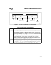
7.3.5.1 Bit Timing Equations
The bit timing equations of the integrated CAN controller are equivalent to those for the 82527
CAN peripheral with the DSC bit in the CPU interface register set (system clock divided by two).
The following equations show the timing calculations for the integrated CAN controller and the
82527 CAN peripheral, respectively.
where:
F
OSC
= the input clock frequency on the XTAL1 pin, in MHz
BRP = the value of the BRP bit in bit timing register 0
TSEG1 = the value of the TSEG1 field in bit timing register 0
TSEG2 = the value of the TSEG1 field in bit timing register 1
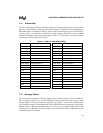
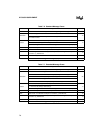
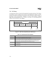
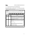
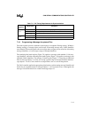
Table 7-10 defines the bit timing relationships of the CAN controller.
Table 7-10. Bit Timing Relationships
Timing
Parameter
Definition
t
BITTIME
t
SYNC_SEG
+ t
TSEG1
+ t
TSEG2
t
XTAL
1
input clock period on XTAL1 (50 ns at 20 MHz operation)
tq 2t
XTAL
1
× (BRP + 1), where BRP is a field in bit timing register 0 (valid values are 0–63)
t
SYNC_SEG
1tq
t
TSEG
1
(TSEG1 + 1) × tq, where TSEG1 is a field in bit timing register 1 (valid values are 2–15)
t
TSEG
2
(TSEG2 + 1) × tq, where TSEG2 is a field in bit timing register 1 (valid values are 1–7)
t
SJW
(SJW + 1) × tq, where SJW is a field in bit timing register 0 (valid values are 0–3)
t
PROP
The portion of t
TSEG
1
that is equivalent to PROP_SEG as defined by the CAN protocol. Twice
the maximum sum of the physical bus delay, input comparator delay, and output driver delay,
rounded up to the nearest multiple of tq.
CAN Controller CAN bus frequency
F
osc
2 BRP + 1()× 3 TSEG1 TSEG2++()×
---------------------------------------------------------------------------------------------------------=
82527 CAN bus frequency
F
osc
DSC 1+()BRP + 1()× 3 TSEG1 TSEG2++()×
---------------------------------------------------------------------------------------------------------------------------------=