


DE2-70 User Manual
38
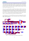
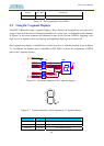
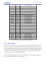
HEX5_D[0] PIN_M3 Seven Segment Digit 5[0]
HEX5_D[1] PIN_L1 Seven Segment Digit 5[1]
HEX5_D[2] PIN_L2 Seven Segment Digit 5[2]
HEX5_D[3] PIN_L3 Seven Segment Digit 5[3]
HEX5_D[4] PIN_K1 Seven Segment Digit 5[4]
HEX5_D[5] PIN_K4 Seven Segment Digit 5[5]
HEX5_D[6] PIN_K5 Seven Segment Digit 5[6]
HEX5_DP PIN_K6 Seven Segment Decimal Point 5
HEX6_D[0] PIN_H6 Seven Segment Digit 6[0]
HEX6_D[1] PIN_H4 Seven Segment Digit 6[1]
HEX6_D[2] PIN_H7 Seven Segment Digit 6[2]
HEX6_D[3] PIN_H8 Seven Segment Digit 6[3]
HEX6_D[4] PIN_G4 Seven Segment Digit 6[4]
HEX6_D[5] PIN_F4 Seven Segment Digit 6[5]
HEX6_D[6] PIN_E4 Seven Segment Digit 6[6]
HEX6_DP PIN_K2 Seven Segment Decimal Point 6
HEX7_D[0] PIN_K3 Seven Segment Digit 7[0]
HEX7_D[1] PIN_J1 Seven Segment Digit 7[1]
HEX7_D[2] PIN_J2 Seven Segment Digit 7[2]
HEX7_D[3] PIN_H1 Seven Segment Digit 7[3]
HEX7_D[4] PIN_H2 Seven Segment Digit 7[4]
HEX7_D[5] PIN_H3 Seven Segment Digit 7[5]
HEX7_D[6] PIN_G1 Seven Segment Digit 7[6]
HEX7_DP PIN_G2 Seven Segment Decimal Point 7
Table 5.4. Pin assignments for the 7-segment displays.
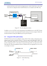
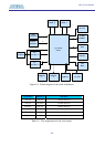
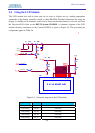
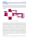
5.4 Clock Circuitry
The DE2-70 board includes two oscillators that produce 28.86 MHz and 50 MHz clock signals.
Both two clock signals are connected to the FPGA that are used for clocking the user logic. Also,
the 28.86 MHz oscillator is used to drive the two TV decoders. The board also includes an SMA
connector which can be used to connect an external clock source to the board. In addition, all these
clock inputs are connected to the phase lock loops (PLL) clock input pin of the FPGA allowed users
can use these clocks as a source clock for the PLL circuit.
The clock distribution on the DE2-70 board is shown in Figure 5.8. The associated pin assignments
for clock inputs to FPGA I/O pins are listed in Table 5.5.