


DE2-70 User Manual
57
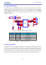
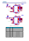
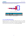
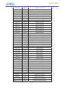
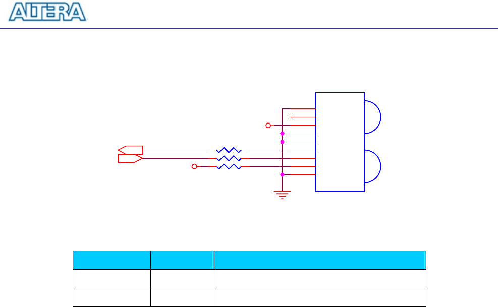
The pin assignments of the associated interface are listed in Table 5.18.
IRDA_TXD
IRDA_RXD
VCC33
VCC33
R42
120
R42
120
R41
120
R41
120
U6
IrDA
U6
IrDA
AGND
4
VCC
3
NC
2
GND
1
SD
5
RXD
6
TXD
7
LEDA
8
SHIELD
9
R43
47
R43
47
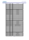
Figure 5.21. IrDA schematic.
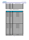
Signal Name FPGA Pin No. Description
IRDA_TXD PIN_W21 IRDA Transmitter
IRDA_RXD PIN_W22 IRDA Receiver
Table 5.18. IrDA pin assignments.
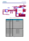
5.16 Using SDRAM/SRAM/Flash
The DE2-70 board provides a 2-Mbyte SSRAM, 8-Mbyte Flash memory, and two 32-Mbyte
SDRAM chips. Figures 5.22, 5.23, and 5.24 show the schematics of the memory chips. The pin
assignments for each device are listed in Tables 5.19, 5.20, and 5.21. The datasheets for the memory
chips are provided in the Datasheet/Memory folder on the DE2-70 System CD-ROM.