


DE2-70 User Manual
45
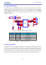
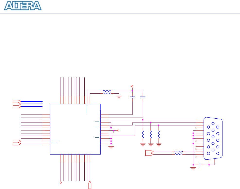
5.7 Using VGA
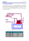
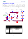
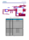
The DE2-70 board includes a 16-pin D-SUB connector for VGA output. The VGA synchronization
signals are provided directly from the Cyclone II FPGA, and the Analog Devices ADV7123 triple
10-bit high-speed video DAC is used to produce the analog data signals (red, green, and blue). The
associated schematic is given in Figure 5.12 and can support resolutions of up to 1600 x 1200 pixels,
at 100 MHz.
RSET
VGA_G9
VGA_G0
VGA_G8
VGA_G7
VGA_G6
VGA_G5
VGA_G4
VGA_G3
V
GA_G2
VGA_G1
VGA_R0
VGA_R1
VGA_R2
VGA_R3
VGA_R4
VGA_R5
VGA_R6
VGA_R7
VGA_R8
VGA_B9
VGA_B8
VGA_B7
VGA_B6
VGA_B5
VGA_B4
VGA_B3
VGA_B2
VGA_B1
VGA_B0
VGA_R9
VGA_B
VGA_R
VGA_G
VGA_BLANK_n
VGA_R[0..9]
VGA_G[0..9]
VGA_B[0..9]
VGA_
SYNC_n
VGA_CLOCK
VGA_HS
VGA_VS
VGA_VCC33
VGA_VCC33
VGA_VCC33
R82
75
R82
75
10
11
6
1
5
15
J7
VG
A
10
11
6
1
5
15
J7
VG
A
5
9
4
8
3
7
2
6
1
17
16
10
11
12
13
14
15
R83
75
R83
75
R84
75
R84
75
BC
49 0.1u
BC
49 0.1u
BC48
0.1u
BC48
0.1u
BC47
0.1u
BC47
0.1u
R81
560
R81
560
R85
47
R85
47
R86
47
R86
47
U10
ADV7123
U10
ADV7123
G6
7
SYNC
12
G1
2
G2
3
B7
21
B8
22
B9
23
CLOCK
24
GND
25
GND
26
IOB
27
IOB
28
B3
17
B4
18
B5
19
B6
20
B2
16
B1
15
B0
14
VAA
13
G0
1
G3
4
BLANK
11
G9
10
G4
5
G5
6
G7
8
G8
9
VAA
29
VAA
30
IOG
31
IOG
32
IOR
33
IOR
34
COMP
35
VREF
36
RSET
37
PSAVE
38
R0
39
R1
40
R2
41
R3
42
R4
43
R5
44
R6
45
R7
46
R8
47
R9
48
R80
4.7K
R80
4.7K
Figure 5.12. VGA circuit schematic.
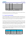
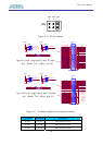
The timing specification for VGA synchronization and RGB (red, green, blue) data can be found on
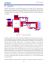
various educational web sites (for example, search for “VGA signal timing”). Figure 5.13 illustrates
the basic timing requirements for each row (horizontal) that is displayed on a VGA monitor. An
active-low pulse of specific duration (time a in the figure) is applied to the horizontal
synchronization (hsync) input of the monitor, which signifies the end of one row of data and the
start of the next. The data (RGB) inputs on the monitor must be off (driven to 0 V) for a time period
called the back porch (b) after the hsync pulse occurs, which is followed by the display interval (c).
During the data display interval the RGB data drives each pixel in turn across the row being
displayed. Finally, there is a time period called the front porch (d) where the RGB signals must
again be off before the next hsync pulse can occur. The timing of the vertical synchronization (vsync)
is the same as shown in Figure 5.13, except that a vsync pulse signifies the end of one frame and the
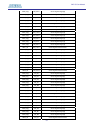
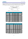
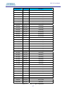
start of the next, and the data refers to the set of rows in the frame (horizontal timing). Table 5.9 and
5.10 show, for different resolutions, the durations of time periods a, b, c, and d for both horizontal
and vertical timing.
Detailed information for using the ADV7123 video DAC is available in its datasheet, which can be