DE2-70 User Manual
81
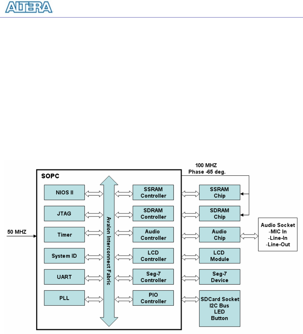
Figure 6.13 shows the hardware block diagram of this demonstration. The system requires a 50
MHZ clock provided from the board. The PLL generates a 100-MHZ clock for NIOS II processor
and the other controllers except for the audio controller. The audio chip is controlled by the Audio
Controller which is a user-defined SOPC component. This audio controller needs an input clock
running at 18.432 MHZ. In this design, the clock is provided by the PLL block. The audio controller
requires the audio chip working in master mode, so the serial bit (BCK) and the left/right channel
clock (LRCK) are provided by the audio chip. The 7-segment display is controlled by the Seg-7
Controller which also is a user-defined SOPC component. Two PIO pins are connected to the I2C
bus. The I2C protocol is implemented by software. Four PIO pins are connected to the SD CARD
socket. SD 1-Bit Mode is used to access the SD card and is implemented by software. All of the
other SOPC components in the block diagram are SOPC Builder built-in components.
Figure 6.13. Block diagram of the SD music player demonstration.
Figure 6.14 shows the software stack of this demonstration. SD 1-Bit Mod block implements the
SD 1-bit mode protocol for reading raw data from the SD card. The FAT16 block implements
FAT16 file system for reading wave files that stored in the SD card. In this block, only read function
is implemented. The WAVE Lib block implements WAVE file decoding function for receiving
audio signal from wave files. The I2C block implements I2C protocol for configuring audio chip.
The SEG7 block implements displaying function for display elapsed playing time. The Audio block
implements audio FIFO checking function and audio signal sending/receiving function.


