


S1C63000 CORE CPU MANUAL EPSON 17
CHAPTER 2: ARCHITECTURE
TOASCII: ;BCD to ASCII conversion
LDB %EXT,0x00 ;Sets address 0040H
LDB %XL,0x40
JR %A
RETD 0x30 ;"0"
RETD 0x31 ;"1"
RETD 0x32 ;"2"
RETD 0x33 ;"3"
RETD 0x34 ;"4"
RETD 0x35 ;"5"
RETD 0x36 ;"6"
RETD 0x37 ;"7"
RETD 0x38 ;"8"
RETD 0x39 ;"9"
As shown in the example, operation results in the A or BA register can simply be converted into other
formats.
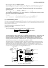
2.3 Data Memory
2.3.1 Configuration of data memory
In addition to the program memory space, the S1C63000 can also access 64K-word (× 4 bits) data memory.
In the individual model of the S1C63 Family, RAM of which size is decided depending on the model and
I/O memory are connected to this space.
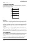
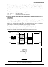
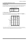
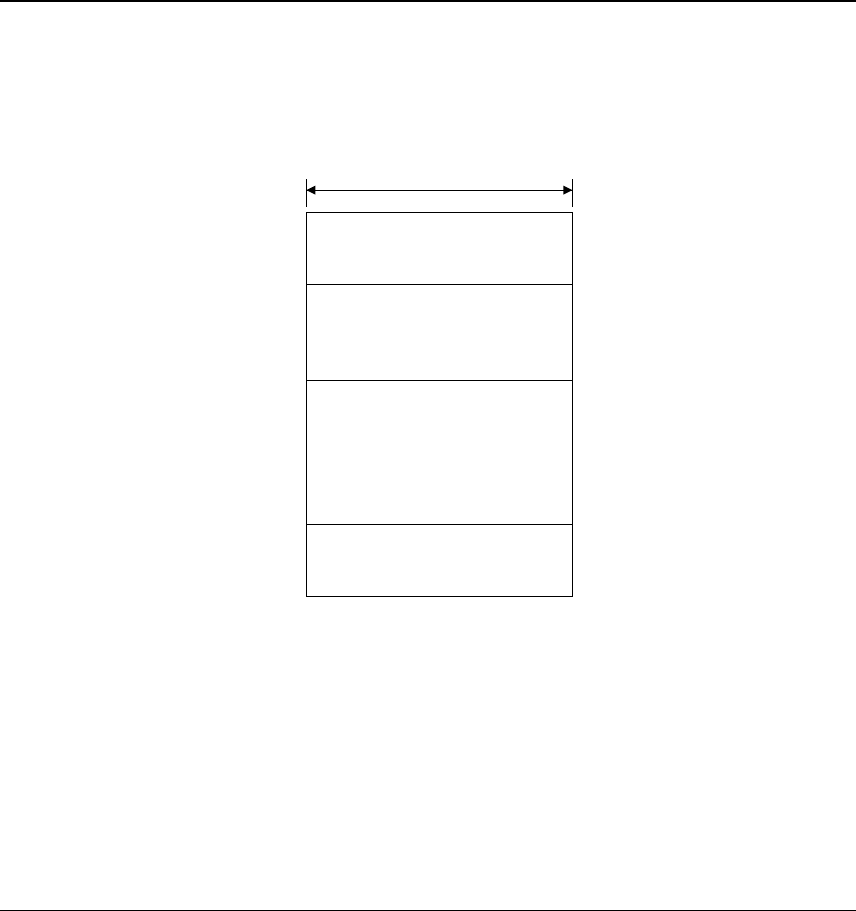
Figure 2.3.1.1 shows the data memory map of the S1C63000.
Fig. 2.3.1.1 S1C63000 data memory map
The S1C63000 can access 64K-word space linearly without any of the page management commonly used
in current 4-bit microcomputers.
The S1C63000 has a built-in 16-bit data bus for the address stack (SP1), and a RAM that permits 16-bit
data accessing can be connected to the addresses 0000H to 03FFH. The 16-bit accessible area is different
depending on the individual models. That area permits normal 4-bit accessing. Switching between 4-bit
accessing and 16-bit accessing is done according to the instruction by the hardware. A normal 4-bit data
stack (SP2) is assigned within the addresses 0000H to 00FFH.
The addresses FF00H to FFFFH are used for an I/O memory area to control the peripheral circuits.
Address
0000H
00FFH
0100H
03FFH
0400H
FEFFH
FF00H
FFFFH
4-bit
Data
and
SP1, SP2 stack area
Data
and
SP1 stack area
Data area
I/O memory area