


2 EPSON S1C63000 CORE CPU MANUAL
CHAPTER 1: OUTLINE
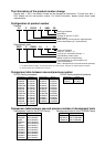
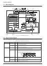
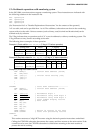
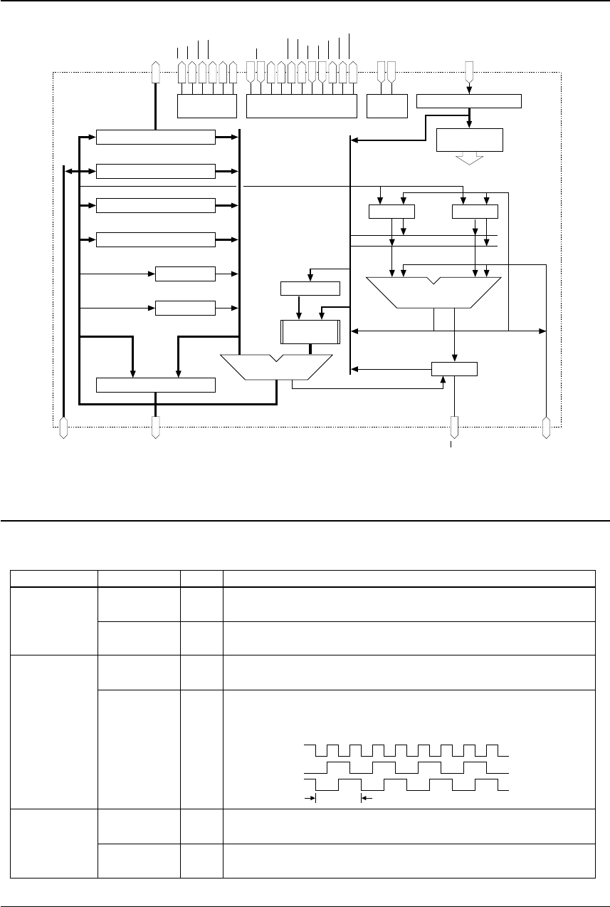
1.3 Block Diagram
Figure 1.3.1 shows the S1C63000 block diagram.
Fig. 1.3.1 S1C63000 block diagram
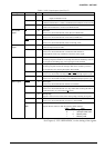
1.4 Input-Output Signals
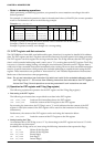
Tables 1.4.1 (a) and 1.4.1 (b) show the input/output signals between the S1C63000 and peripheral circuits.
Table 1.4.1(a) Input/output signal list (1)
Type I/O
I
I
I
O
O
O
FunctionTerminal name
Power supply
Clock
Address bus
V
DD
(V
D1
)
V
SS
(V
S1
)
CLK
PK
PL
IA00–IA15
DA00–DA15
Power supply (+)
Inputs a plus supply voltage.
Power supply (-)
Inputs a minus supply voltage.
Clock input
Inputs the system clock from the peripheral circuit.
2-phase divided clock output
Outputs the 2-phase divided signals to be generated from the system clock
input to the CLK terminal as following phase.
Instruction address output
Outputs an instruction (code ROM) address.
Data address output
Outputs a data (RAM, I/O) address.
CLK
PK
PL
1 cycle
PC (16)
QUEUE (16)
X (16)
Y (16)
SP2 (8)
SP1 (8)
DATA ADDRESS LATCH
A (4)
F (4)
Port A Port B
4-bit ALU
B (4)
Port A Port B
16-bit ADDER
EXT (8)
ADDRESS
OPERATOR
BUS
CONTROL
TIMING & INTERRUPT
CONTROL
POWER
SUPPLY
RD
WR
RDIV
BS16
DBS0
DBS1
CLK
SR
PK
PL
STOP
USLP
IRQ
NMI
IACK
NACK
FETCH
V
DD
V
SS
IR (13)
INSTRUCTION
DECODER
µ Instruction
IA00
–IA15
I00
–I12
M00
–M15
DA00
–DA15
IF
D0
–D3
S1C63000